In general, semiconductors are materials, inorganic or organic, which have the ability to control their conduction depending on chemical structure, temperature, illumination, and presence of dopants. The name semiconductor comes from the fact that these materials have an electrical conductivity between that of a metal, like copper, gold, etc. and an insulator, such as glass. They have an energy gap less than 4eV (about 1eV). In solid-state physics, this energy gap or band gap is an energy range between valence band and conduction band where electron states are forbidden. In contrast to conductors, electrons in a semiconductor must obtain energy (e.g. from ionizing radiation) to cross the band gap and to reach the conduction band. Properties of semiconductors are determined by the energy gap between valence and conduction bands.
Extrinsic Semiconductors – Doped Semiconductors
An extrinsic semiconductor, or doped semiconductor, is a semiconductor, that was intentionally doped for the purpose of modulating its electrical, optical and structural properties. In case of semiconductor detectors of ionizing radiation, doping is the intentional introduction of impurities into an intrinsic semiconductor for the purpose of changes in their electrical properties. Therefore, intrinsic semiconductors are also known as pure semiconductors or i-type semiconductors.
The addition of a small percentage of foreign atoms in the regular crystal lattice of silicon or germanium produces dramatic changes in their electrical properties, since these foreign atoms incorporated into the crystal structure of the semiconductor provide free charge carriers (electrons or electron holes) in the semiconductor. In an extrinsic semiconductor it is these foreign dopant atoms in the crystal lattice that mainly provide the charge carriers which carry electric current through the crystal. In general, there are two types of dopant atoms resulting in two types of extrinsic semiconductors. These dopants that produce the desired controlled changes are classified as either electron acceptors or donors and the corresponding doped semiconductors are known as:
- n-type Semiconductors.
- p-type Semiconductors.
Extrinsic semiconductors are components of many common electrical devices, as well of many detectors of ionizing radiation. For these purpose, a semiconductor diode (devices that allow current in only one direction) usually consists of p-type and n-type semiconductors placed in junction with one another.
n-type Semiconductors
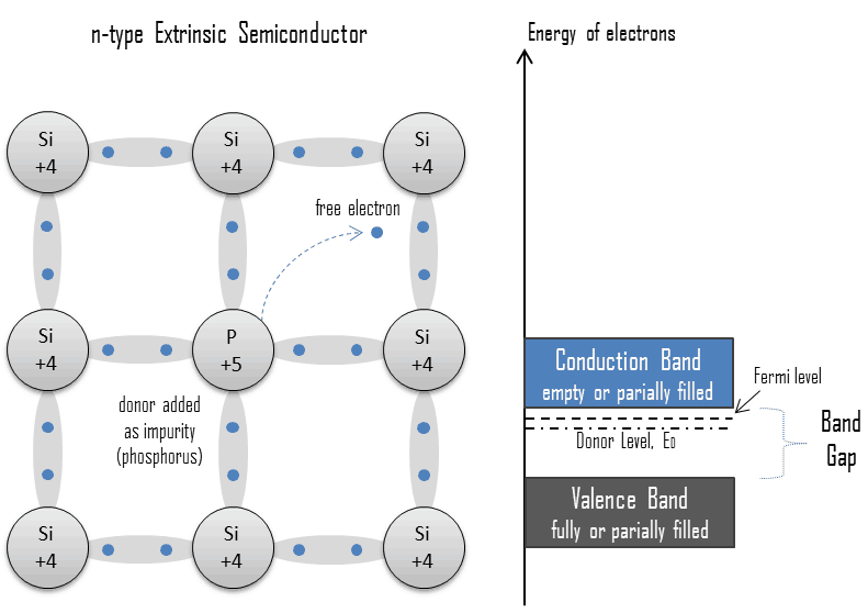 An extrinsic semiconductor which has been doped with electron donor atoms is called an n-type semiconductor, because the majority of charge carriers in the crystal are negative electrons. Since silicon is a tetravalent element, the normal crystal structure contains 4 covalent bonds from four valence electrons. In silicon, the most common dopants are group III and group V elements. Group V elements (pentavalent) have five valence electrons, which allows them to act as a donor. That means, the addition of these pentavalent impurities such as arsenic, antimony or phosphorus contributes free electrons, greatly increasing the conductivity of the intrinsic semiconductor. For example, a silicon crystal doped with boron (group III) creates a p-type semiconductor whereas a crystal doped with phosphorus (group V) results in an n-type semiconductor.
The conduction electrons are completely dominated by the number of donor electrons. Therefore:
The total number of conduction electrons is approximately equal to the number of donor sites, n≈ND.
Charge neutrality of semiconductor material is maintained because excited donor sites balance the conduction electrons. The net result is that the number of conduction electrons is increased, while the number of holes is reduced. The imbalance of the carrier concentration in the respective bands is expressed by the different absolute number of electrons and holes. Electrons are majority carriers, while holes are minority carriers in n-type material.
p-type Semiconductors
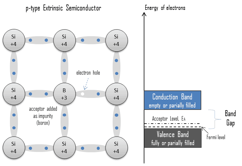 An extrinsic semiconductor which has been doped with electron acceptor atoms is called a p-type semiconductor, because the majority of charge carriers in the crystal are electron holes (positive charge carriers). The pure semiconductor silicon is a tetravalent element, the normal crystal structure contains 4 covalent bonds from four valence electrons. In silicon, the most common dopants are group III and group V elements. Group III elements (trivalent) all contain three valence electrons, causing them to function as acceptors when used to dope silicon. When an acceptor atom replaces a tetravalent silicon atom in the crystal, a vacant state (an electron hole) is created. An electron hole (often simply called a hole) is the lack of an electron at a position where one could exist in an atom or atomic lattice. It is one of the two types of charge carriers that are responsible for creating electric current in semiconducting materials. These positively charged holes can move from atom to atom in semiconducting materials as electrons leave their positions. The addition of trivalent impurities such as boron, aluminum or gallium to an intrinsic semiconductor creates these positive electron holes in the structure. For example, a silicon crystal doped with boron (group III) creates a p-type semiconductor whereas a crystal doped with phosphorus (group V) results in an n-type semiconductor.
The number of electron holes are completely dominated by the number of acceptor sites. Therefore:
The total number of holes is approximately equal to the number of donor sites, p ≈ NA.
Charge neutrality of this semiconductor material is also maintained. The net result is that the number of electron holes is increased, while the number of conduction electrons is reduced. The imbalance of the carrier concentration in the respective bands is expressed by the different absolute number of electrons and holes. Electron holes are majority carriers, while electrons are minority carriers in p-type material.
The P-N Junction – Reverse Biased Junction
The semiconductor detector operates much better as a radiation detector if an external voltage is applied across the junction in the reverse biased direction. The depletion region will function as a radiation detector. Improvement can be reached by use of a reverse-bias voltage to the P-N junction to deplete the detector of free carriers, which is the principle of the most semiconductor detectors. Reverse biasing a junction increases the thickness of the depletion region because the potential difference across the junction is enhanced. Germanium detectors have a p-i-n structure in which the intrinsic (i) region is sensitive to ionizing radiation, particularly X rays and gamma rays. Under reverse bias, an electric field extends across the intrinsic or depleted region. In this case, negative voltage is applied to the p-side and positive to the second one. Holes in the p-region are attracted from the junction towards the p contact and similarly for electrons and the n contact. This charge, which is in proportion to the energy deposited in the detector by the incoming photon, is converted into a voltage pulse by an integral charge sensitive preamplifier.
See also: Germanium Detectors, MIRION Technologies. <available from: https://www.mirion.com/products/germanium-detectors>.
We hope, this article, Extrinsic Semiconductor – Doped Semiconductor, helps you. If so, give us a like in the sidebar. Main purpose of this website is to help the public to learn some interesting and important information about radiation and dosimeters.