An annihilation peak may be observed for high energy gamma rays (greater than 1.02 MeV), where electron-positron pair production is a possible interaction. Radiation Dosimetry
Analysis of gamma spectra is very interesting, since it has a structure and workers must distinguish between true pulses to be analyzed and accompanying pulses from different sources of radiation. We will show the structure of the gamma spectrum on the example of cobalt-60 measured by NaI(Tl) scintillation detector and by the HPGe detector. The HPGe detector allows the separation of many closely spaced gamma lines, which is very beneficial for measuring multi-gamma emitting radioactive sources.
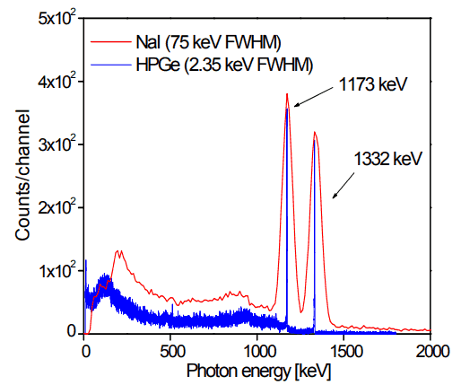
Cobalt-60 is an artificial radioactive isotope of cobalt with a half-life of 5.2747 years. It is synthetically produced by neutron activation of cobalt-59 in nuclear reactors. Cobalt-60 is a common calibration source found in many laboratories. The gamma spectrum has two significant peaks, one at 1173.2 keV and another at 1332.5 keV. Good scintillation detectors should have adequate resolution to separate the two peaks. For HPGe detectors, these peaks are perfectly separated.
As can be seen from the figure, there are two gamma ray photopeaks. Both detectors also show response at the lower energies, caused by Compton scattering, two smaller escape peaks at energies 0.511 and 1.022 MeV below the photopeak for the creation of electron-positron pairs when one or both annihilation photons escape, and a backscatter peak. Higher energies can be measured when two or more photons strike the detector almost simultaneously, appearing as sum peaks with energies up to the value of two or more photopeaks added.
Figure: Caption: Comparison of NaI(Tl) and HPGe spectra for cobalt-60. Source: Radioisotopes and Radiation Methodology I, II. Soo Hyun Byun, Lecture Notes. McMaster University, Canada.
Annihilation Peak
For high energy gamma rays (greater than 1.02 MeV), electron-positron pair production is a possible interaction. But a positron may then annihilate in the detector or in the surrounding material. If both 0.51 MeV annihilation photons are absorbed in the crystal, a secondary peak 1.02 MeV below the photopeak can be found. If one annihilation photon is absorbed and the second exits the crystal, then 0.51 MeV is removed from the photopeak, resulting in a secondary peak 0.51 MeV below the photopeak. The probability is greater that one annihilation photon will be absorbed.
Robert Reed Burn, Introduction to Nuclear Reactor Operation, 1988.
U.S. Department of Energy, Nuclear Physics and Reactor Theory. DOE Fundamentals Handbook, Volume 1 and 2. January 1993.
Paul Reuss, Neutron Physics. EDP Sciences, 2008. ISBN: 978-2759800414.
See also:
Gamma Spectroscopy
We hope, this article, Annihilation Peak – Spectrum, helps you. If so, give us a like in the sidebar. Main purpose of this website is to help the public to learn some interesting and important information about radiation and dosimeters.
Coincidence peak may be observed, when simultaneous absorption of two gamma photons in crystal occurs. It results in a peak higher in energy than the photopeak. Radiation Dosimetry
Analysis of gamma spectra is very interesting, since it has a structure and workers must distinguish between true pulses to be analyzed and accompanying pulses from different sources of radiation. We will show the structure of the gamma spectrum on the example of cobalt-60 measured by NaI(Tl) scintillation detector and by the HPGe detector. The HPGe detector allows the separation of many closely spaced gamma lines, which is very beneficial for measuring multi-gamma emitting radioactive sources.
Cobalt-60 is an artificial radioactive isotope of cobalt with a half-life of 5.2747 years. It is synthetically produced by neutron activation of cobalt-59 in nuclear reactors. Cobalt-60 is a common calibration source found in many laboratories. The gamma spectrum has two significant peaks, one at 1173.2 keV and another at 1332.5 keV. Good scintillation detectors should have adequate resolution to separate the two peaks. For HPGe detectors, these peaks are perfectly separated.
As can be seen from the figure, there are two gamma ray photopeaks. Both detectors also show response at the lower energies, caused by Compton scattering, two smaller escape peaks at energies 0.511 and 1.022 MeV below the photopeak for the creation of electron-positron pairs when one or both annihilation photons escape, and a backscatter peak. Higher energies can be measured when two or more photons strike the detector almost simultaneously, appearing as sum peaks with energies up to the value of two or more photopeaks added.
Figure: Caption: Comparison of NaI(Tl) and HPGe spectra for cobalt-60. Source: Radioisotopes and Radiation Methodology I, II. Soo Hyun Byun, Lecture Notes. McMaster University, Canada.
Coincidence Peak
Simultaneous absorption of two gamma photons in crystal, resulting in a peak higher in energy than the photopeak. The gamma photons may result from serial isomeric transitions (e.g. 2 keV plus 1332.5 keV in case of cobalt-60) or simultaneous decays in separate radionuclides (e.g. 2 x 1173.2 keV in case of cobalt-60).
Robert Reed Burn, Introduction to Nuclear Reactor Operation, 1988.
U.S. Department of Energy, Nuclear Physics and Reactor Theory. DOE Fundamentals Handbook, Volume 1 and 2. January 1993.
Paul Reuss, Neutron Physics. EDP Sciences, 2008. ISBN: 978-2759800414.
See also:
Gamma Spectroscopy
We hope, this article, Coincidence Peak – Spectrum, helps you. If so, give us a like in the sidebar. Main purpose of this website is to help the public to learn some interesting and important information about radiation and dosimeters.
For small detectors the chance for a photon to leave after Compton scattering is high and the Compton continuum would be large compared to the photopeak. Radiation Dosimetry
Analysis of gamma spectra is very interesting, since it has a structure and workers must distinguish between true pulses to be analyzed and accompanying pulses from different sources of radiation. We will show the structure of the gamma spectrum on the example of cobalt-60 measured by NaI(Tl) scintillation detector and by the HPGe detector. The HPGe detector allows the separation of many closely spaced gamma lines, which is very beneficial for measuring multi-gamma emitting radioactive sources.
Cobalt-60 is an artificial radioactive isotope of cobalt with a half-life of 5.2747 years. It is synthetically produced by neutron activation of cobalt-59 in nuclear reactors. Cobalt-60 is a common calibration source found in many laboratories. The gamma spectrum has two significant peaks, one at 1173.2 keV and another at 1332.5 keV. Good scintillation detectors should have adequate resolution to separate the two peaks. For HPGe detectors, these peaks are perfectly separated.
As can be seen from the figure, there are two gamma ray photopeaks. Both detectors also show response at the lower energies, caused by Compton scattering, two smaller escape peaks at energies 0.511 and 1.022 MeV below the photopeak for the creation of electron-positron pairs when one or both annihilation photons escape, and a backscatter peak. Higher energies can be measured when two or more photons strike the detector almost simultaneously, appearing as sum peaks with energies up to the value of two or more photopeaks added.
Figure: Caption: Comparison of NaI(Tl) and HPGe spectra for cobalt-60. Source: Radioisotopes and Radiation Methodology I, II. Soo Hyun Byun, Lecture Notes. McMaster University, Canada.
Compton Continuum
In the crystal, a gamma ray undergoes a number of interactions, but for intermediate energies compton scattering dominates. In compton scattering, the incident gamma ray photon is deflected through an angle Θ with respect to its original direction. The photon transfers a portion of its energy to the recoil electron. The energy transferred to the recoil electron can vary from zero to a large fraction (maximum E) of the incident gamma ray energy, because all angles of scattering are possible. The size of the scintillation crystal changes the ratio between photopeak and Compton continuum. For an infinitely large spherical detector centered around a source no photons would be able to escape and only a photopeak would be seen on the spectrum. For very small detectors the chance for a photon to leave after Compton scattering is high and the Compton continuum would be large compared to the photopeak.
Compton Edge
The Compton edge is a feature of the spectrograph that results from the Compton scattering in the scintillator or detector. This feature is due to photons that undergo Compton scattering with a scattering angle of 180° and then escape the detector. When a gamma ray scatters off the detector and escapes, only a fraction of its initial energy can be deposited in the sensitive layer of the detector. It depends on the scattering angle of the photon, how much energy will be deposited in the detector. This leads to a spectrum of energies. The Compton edge energy corresponds to full backscattered photon. The counts between Compton edge and the photopeaks are caused by multiple Compton scattering events, where scattered gamma photon exits the sensitive material.
Robert Reed Burn, Introduction to Nuclear Reactor Operation, 1988.
U.S. Department of Energy, Nuclear Physics and Reactor Theory. DOE Fundamentals Handbook, Volume 1 and 2. January 1993.
Paul Reuss, Neutron Physics. EDP Sciences, 2008. ISBN: 978-2759800414.
See also:
Gamma Spectroscopy
We hope, this article, Compton Continuum – Compton Plateau – Spectrum, helps you. If so, give us a like in the sidebar. Main purpose of this website is to help the public to learn some interesting and important information about radiation and dosimeters.
This gives an characteristic X-ray peak with an energy depending on the material it came from. In case of lead the characteristic X-ray energies is in the 72-84 keV range. Radiation Dosimetry
Analysis of gamma spectra is very interesting, since it has a structure and workers must distinguish between true pulses to be analyzed and accompanying pulses from different sources of radiation. We will show the structure of the gamma spectrum on the example of cobalt-60 measured by NaI(Tl) scintillation detector and by the HPGe detector. The HPGe detector allows the separation of many closely spaced gamma lines, which is very beneficial for measuring multi-gamma emitting radioactive sources.
Cobalt-60 is an artificial radioactive isotope of cobalt with a half-life of 5.2747 years. It is synthetically produced by neutron activation of cobalt-59 in nuclear reactors. Cobalt-60 is a common calibration source found in many laboratories. The gamma spectrum has two significant peaks, one at 1173.2 keV and another at 1332.5 keV. Good scintillation detectors should have adequate resolution to separate the two peaks. For HPGe detectors, these peaks are perfectly separated.
As can be seen from the figure, there are two gamma ray photopeaks. Both detectors also show response at the lower energies, caused by Compton scattering, two smaller escape peaks at energies 0.511 and 1.022 MeV below the photopeak for the creation of electron-positron pairs when one or both annihilation photons escape, and a backscatter peak. Higher energies can be measured when two or more photons strike the detector almost simultaneously, appearing as sum peaks with energies up to the value of two or more photopeaks added.
Figure: Caption: Comparison of NaI(Tl) and HPGe spectra for cobalt-60. Source: Radioisotopes and Radiation Methodology I, II. Soo Hyun Byun, Lecture Notes. McMaster University, Canada.
X-ray Peaks
When the gamma rays undergoes photoelectric effect in surrounding materials (for example lead shield) the outgoing X-ray can be captured again by the detector. This gives an characteristic X-ray peak with an energy depending on the material it came from. In case of lead the characteristic X-ray energies is in the 72-84 keV range. Photoelectric absorption by K-shell electron in lead of shielding, resulting in a K-shell vacancy. The K -> L transition for lead = 72 keV. If this characteristic x-ray is absorbed in the crystal then a secondary peak at 72 keV is observed.
Robert Reed Burn, Introduction to Nuclear Reactor Operation, 1988.
U.S. Department of Energy, Nuclear Physics and Reactor Theory. DOE Fundamentals Handbook, Volume 1 and 2. January 1993.
Paul Reuss, Neutron Physics. EDP Sciences, 2008. ISBN: 978-2759800414.
See also:
Gamma Spectroscopy
We hope, this article, X-Ray Peak – Spectrum, helps you. If so, give us a like in the sidebar. Main purpose of this website is to help the public to learn some interesting and important information about radiation and dosimeters.
Properties of semiconductors are determined by the energy gap between valence and conduction bands. To understand, what is semiconductor, we have to define these terms. Radiation Dosimetry
In general, semiconductors are materials, inorganic or organic, which have the ability to control their conduction depending on chemical structure, temperature, illumination, and presence of dopants. The name semiconductor comes from the fact that these materials have an electrical conductivity between that of a metal, like copper, gold, etc. and an insulator, such as glass. They have an energy gap less than 4eV (about 1eV). In solid-state physics, this energy gap or band gap is an energy range between valence band and conduction band where electron states are forbidden. In contrast to conductors, electrons in a semiconductor must obtain energy (e.g. from ionizing radiation) to cross the band gap and to reach the conduction band. Properties of semiconductors are determined by the energy gap between valence and conduction bands. To understand, what is semiconductor, we have to define these terms.
Properties of Semiconductors
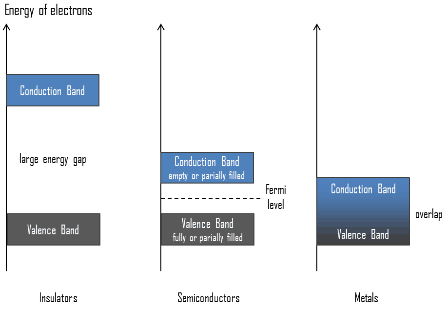
To understand the difference between metals, semiconductors and electrical insulators, we have to define the following terms from solid-state physics:
Valence Band. In solid-state physics, the valence band and conduction band are the bands closest to the Fermi level and thus determine the electrical conductivity of the solid. In electrical insulators and semiconductors, the valence band is the highest range of electron energies in which electrons are normally present at absolute zero temperature. For example, a silicon atom has fourteen electrons. In the ground state, they are arranged in the electron configuration [Ne]3s23p2. Of these, four are valence electrons, occupying the 3s orbital and two of the 3p orbitals. The distinction between the valence and conduction bands is meaningless in metals, because conduction occurs in one or more partially filled bands that take on the properties of both the valence and conduction bands.
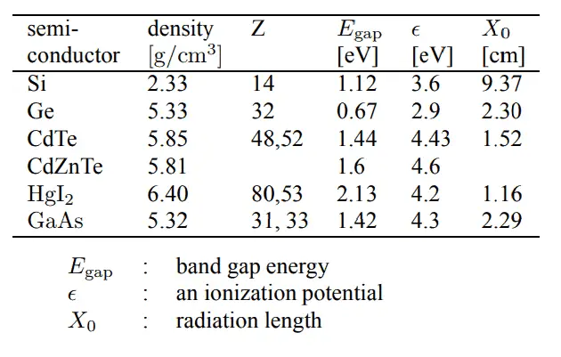
Conduction Band. In solid-state physics, the valence band and conduction band are the bands closest to the Fermi level and thus determine the electrical conductivity of the solid. In electrical insulators and semiconductors, the conduction band is the lowest range of vacant electronic states. On a graph of the electronic band structure of a material, the valence band is located below the Fermi level, while the conduction band is located above it. In semiconductors, electrons may reach the conduction band, when they are excited, for example, by ionizing radiation (i.e. they must obtain energy higher than Egap). For example, diamond is a wide-band gap semiconductor (Egap = 5.47 eV) with high potential as an electronic device material in many devices. On the other side, germanium has a small band gap energy (Egap = 0.67 eV), which requires to operate the detector at cryogenic temperatures. The distinction between the valence and conduction bands is meaningless in metals, because conduction occurs in one or more partially filled bands that take on the properties of both the valence and conduction bands.
Band Gap. In solid-state physics, the energy gap or the band gap is an energy range between valence band and conduction band where electron states are forbidden. In contrast to conductors, electrons in a semiconductor must obtain energy (e.g. from ionizing radiation) to cross the band gap and to reach the conduction band. Band gaps are naturally different for different materials. For example, diamond is a wide-band gap semiconductor (Egap = 5.47 eV) with high potential as an electronic device material in many devices. On the other side, germanium has a small band gap energy (Egap = 0.67 eV), which requires to operate the detector at cryogenic temperatures.
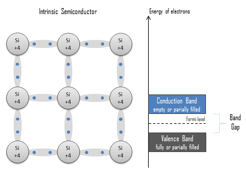
Fermi Level. The term “Fermi level” comes from Fermi-Dirac statistics, which describes a distribution of particles over energy states in systems consisting of fermions (electrons) that obey the Pauli exclusion principle. Since they cannot exist in identical energy states, Fermi level is the term used to describe the top of the collection of electron energy levels at absolute zero temperature. The Fermi level is the surface of Fermi sea at absolute zero where no electrons will have enough energy to rise above the surface. In metals, the Fermi level lies in the hypothetical conduction band giving rise to free conduction electrons. In semiconductors the position of the Fermi level is within the band gap, approximately in the middle of the band gap.
Electron-hole Pair. In the semiconductor, free charge carriers are electrons and electron holes (electron-hole pairs). Electrons and holes are created by excitation of electron from valence band to the conduction band. An electron hole (often simply called a hole) is the lack of an electron at a position where one could exist in an atom or atomic lattice. It is one of the two types of charge carriers that are responsible for creating electric current in semiconducting materials. Since in a normal atom or crystal lattice the negative charge of the electrons is balanced by the positive charge of the atomic nuclei, the absence of an electron leaves a net positive charge at the hole’s location. Positively charged holes can move from atom to atom in semiconducting materials as electrons leave their positions. When an electron meets with a hole, they recombine and these free carriers effectively vanish. The recombination means an electron which has been excited from the valence band to the conduction band falls back to the empty state in the valence band, known as the holes.
The conductivity of a semiconductor can be modeled in terms of the band theory of solids. The band model of a semiconductor suggests that at ordinary temperatures there is a finite possibility that electrons can reach the conduction band and contribute to electrical conduction. In the semiconductor, free charge carriers (electron-hole pairs) are created by excitation of electron from valence band to the conduction band. This excitation left a hole in the valence band which behaves as positive charge and an electron-hole pair is created. Holes can sometimes be confusing as they are not physical particles in the way that electrons are, rather they are the absence of an electron in an atom. Holes can move from atom to atom in semiconducting materials as electrons leave their positions.
Electron Excitation in Semiconductors
Energy for the excitation can be obtained by different ways.
Thermal Excitation
Electron-hole pairs are constantly generated from thermal energy as well, in the absence of any external energy source. Thermal excitation does not require any other form of starting impulse. This phenomenon occurs also at room temperature. It is caused by impurities, irregularity in structure lattice or by dopant. It strongly depends on the Egap (a distance between valence and conduction band), so that for lower Egap a number of thermally excited charge carriers increases. Since thermal excitation results in the detector noise, active cooling is required for some types of semiconductors (e.g. germanium). Detectors based on silicon have sufficiently low noise even by room temperature. This is caused by the large band gap of silicon (Egap= 1.12 eV), which allows us to operate the detector at room temperature, but cooling is prefered to reduce noise.
Optical Excitation
Note that, energy of a single photon of visible light spectrum is comparable with these band gaps. Photons of wave lengths 700 nm – 400 nm have energies of 1.77 eV 3.10 eV. As a result, also visible light is able to excite electrons to the conduction band. Actually, this is the principle of photovoltaic panels that generate electric current.
Excitation by Ionizing Radiation
Electrons may reach the conduction band, when they are excited by ionizing radiation (i.e. they must obtain energy higher than Egap). In general, heavy charged particles transfer energy mostly by:
Excitation. The charged particle can transfer energy to the atom, raising electrons to a higher energy levels.
Ionization. Ionization can occur, when the charged particle have enough energy to remove an electron. This results in a creation of ion pairs in surrounding matter.
A convenient variable that describes the ionization properties of surrounding medium is the stopping power. The classical expression that describes the specific energy loss is known as the Bethe formula. For alpha particles and heavier particles the stopping power of most materials is very high for heavy charged particles and these particles have very short ranges.
In addition to these interactions, beta particles also lose energy by radiative process known as the bremsstrahlung. From classical theory, when a charged particle is accelerated or decelerated, it must radiate energy and the deceleration radiation is known as the bremsstrahlung (“braking radiation”).
Photons (gamma rays and X-rays) can ionize atoms directly (despite they are electrically neutral) through the Photoelectric effect and the Compton effect, but secondary (indirect) ionization is much more significant. Although a large number of possible interactions are known, there are three key interaction mechanisms with matter.
In all cases, a particle of ionizing radiation deposits a portion of its energy along its path. Particle passing through the detector ionizes the atoms of semiconductor, producing the electron-hole pairs. For example, typical thickness of silicon detector is about 300 µm so the number of generated electron-hole pairs by minimum ionizing particle (MIP) passing perpendicular through the detector is about 3.2 x 10⁴. This value is minor in comparison the total number of free carriers in intrinsic semiconductor of a surface of 1 cm2 and the same thickness. Note that, a sample of pure germanium at 20 °C contains about 1.26×10²¹ atoms, but also contains 7.5 x 10¹¹ free electrons and 7.5 x 10¹¹ holes constantly generated from thermal energy. As can be seen, the signal to noise ratio (S/N) would be minimal. The addition of 0.001% of arsenic (an impurity) donates an extra 1015 free electrons in the same volume and the electrical conductivity is increased by a factor of 10,000. In doped material the signal to noise ratio (S/N) would be even smaller. Cooling of the semiconductor is one way to lower this ratio.
Improvement can be reached by use of a reverse-bias voltage to the P-N junction to deplete the detector of free carriers, which is the principle of the most silicon radiation detectors. In this case, negative voltage is applied to the p-side and positive to the second one. Holes in the p-region are attracted from the junction towards the p contact and similarly for electrons and the n contact.
Robert Reed Burn, Introduction to Nuclear Reactor Operation, 1988.
U.S. Department of Energy, Nuclear Physics and Reactor Theory. DOE Fundamentals Handbook, Volume 1 and 2. January 1993.
Paul Reuss, Neutron Physics. EDP Sciences, 2008. ISBN: 978-2759800414.
See also:
Semiconductor Detectors
We hope, this article, Semiconductor – Properties of Semiconductors, helps you. If so, give us a like in the sidebar. Main purpose of this website is to help the public to learn some interesting and important information about radiation and dosimeters.
There are many types of semiconductors in nature and others synthesized in laboratories; however, the best known are silicon (Si) and germanium (Ge). Radiation Dosimetry
In general, semiconductors are materials, inorganic or organic, which have the ability to control their conduction depending on chemical structure, temperature, illumination, and presence of dopants. The name semiconductor comes from the fact that these materials have an electrical conductivity between that of a metal, like copper, gold, etc. and an insulator, such as glass. They have an energy gap less than 4eV (about 1eV). In solid-state physics, this energy gap or band gap is an energy range between valence band and conduction band where electron states are forbidden. In contrast to conductors, electrons in a semiconductor must obtain energy (e.g. from ionizing radiation) to cross the band gap and to reach the conduction band. Properties of semiconductors are determined by the energy gap between valence and conduction bands.
Types of Semiconductors
Semiconductor Materials
There are many types of semiconductors in nature and others synthesized in laboratories; however, the best known are silicon (Si) and germanium (Ge).
Types of semiconductors:
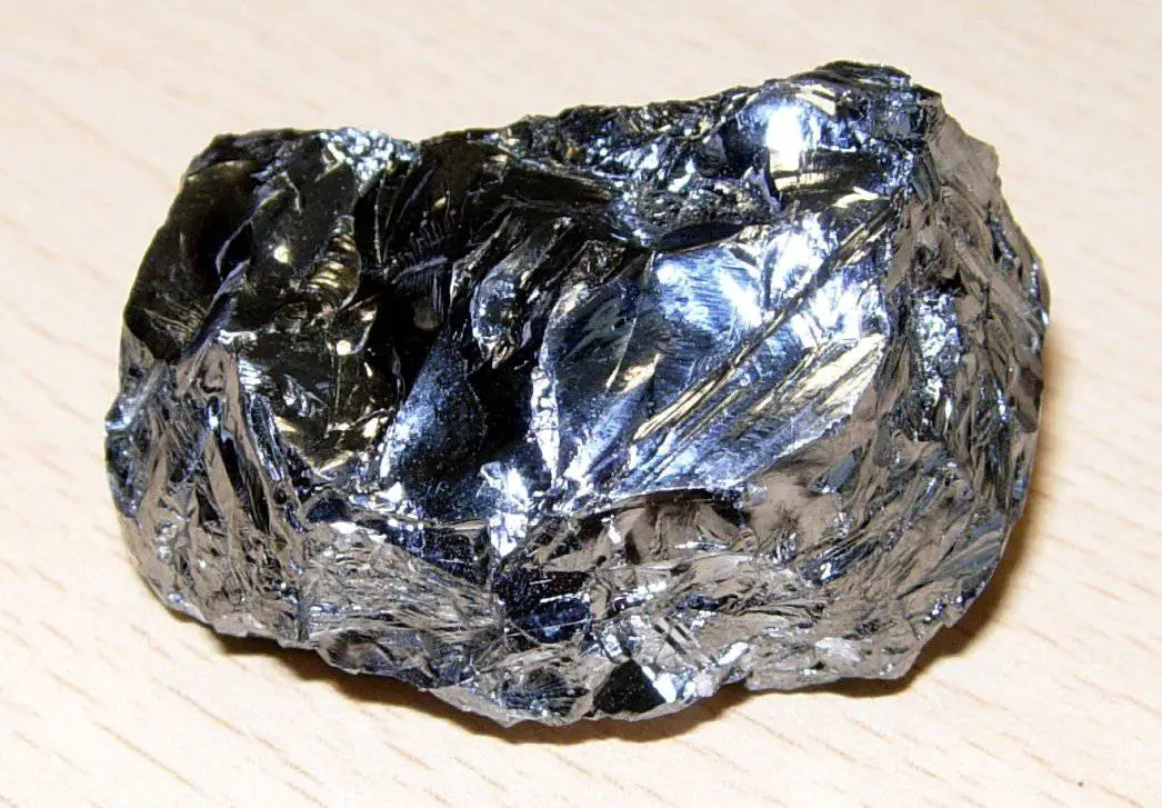
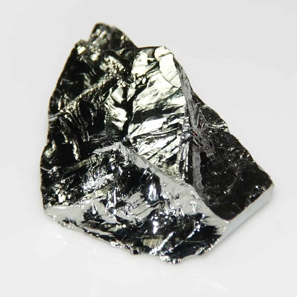
Purified silicon. Source: wikipedia.org License: Public Domain
Silicon. Silicon is a chemical element with atomic number14 which means there are 14 protons and 14 electrons in the atomic structure. The chemical symbol for Silicon is Si. Silicon is a hard and brittle crystalline solid with a blue-grey metallic lustre, it is a tetravalent metalloid and semiconductor. Silicon is mainly used for charged particle detectors (especially for tracking charged particles) and soft X-ray detectors. The large band-gap energy (Egap= 1.12 eV) allows us to operate the detector at room temperature, but cooling is prefered to reduce noise. Silicon based detectors are very important in high-energy physics. Since silicon-based detectors are very good for tracking charged particles, they constitute a substantial part of detection system at the LHC in CERN.
12 grams polycrystalline germanium. Source: wikipedia.org License: CC BY 3.0
Germanium. Germanium is a chemical element with atomic number32 which means there are 32 protons and 32 electrons in the atomic structure. The chemical symbol for Germanium is Ge. Germanium is a lustrous, hard, grayish-white metalloid in the carbon group, chemically similar to its group neighbors tin and silicon. Pure germanium is a semiconductor with an appearance similar to elemental silicon. Germanium is widely used for gamma ray spectroscopy. In gamma spectroscopy, germanium is preferred due to its atomic number being much higher than silicon and which increases the probability of gamma ray interaction. Germanium is more used than silicon for radiation detection because the average energy necessary to create an electron-hole pair is 3.6 eV for silicon and 2.9 eV for germanium, which provides the latter a better resolution in energy. On the other hand, germanium has a small band gap energy (Egap = 0.67 eV), which requires to operate the detector at cryogenic temperatures.
Diamond. Diamond is a solid form of the element carbon with its atoms arranged in a crystal structure called diamond cubic. Diamonds are also very good electrical insulators which strangely is both useful and problematic for electrical devices. Diamond is a wide-band gap semiconductor (Egap= 5.47 eV) with high potential as an electronic device material in many devices. Diamond detectors have many similarities with silicon detectors, but are expected to offer significant advantages, in particular a high radiation hardness and very low drift currents.
CdTe and CdZnTe. Cadmium telluride (CdTe) and cadmium zinc telluride (CdZnTe) have been regarded as promising semiconductor materials for hard X-ray and gamma ray detection. The high atomic number and the high density of these materials mean they can effectively attenuate X-rays and gamma rays with energies of greater than 20 keV that traditional silicon-based sensors are unable to detect. This significantly increases their quantum efficiency in comparison with silicon-based . The large band-gap energy (Egap= 1.44 eV) allows us to operate the detector at room temperature. On the other hand, a considerable amount of charge loss in these detectors produces a reduced energy resolution.
Intrinsic Semiconductor – Pure Semiconductor
An intrinsic semiconductor is completely pure semiconductor without any significant dopant species present. Therefore, intrinsic semiconductors are also known as pure semiconductors or i-type semiconductors.
The number of charge carriers at certain temperature is therefore determined by the properties of the material itself instead of the amount of impurities. Note that, a 1 cm3 sample of pure germanium at 20 °C contains about 4.2×10²² atoms, but also contains about 2.5 x 10¹³ free electrons and 2.5 x 10¹³ holes. These charge carriers are produced by thermal excitation. In intrinsic semiconductors, the number of excited electrons and the number of holes are equal: n = p. Electrons and holes are created by excitation of electron from valence band to the conduction band. An electron hole (often simply called a hole) is the lack of an electron at a position where one could exist in an atom or atomic lattice. This equality may even be the case after doping the semiconductor, though only if it is doped with both donors and acceptors equally. In this case, n = p still holds, and the semiconductor remains intrinsic, though doped.
Semiconductors have an energy gap less than 4eV (about 1eV). Band gaps are naturally different for different materials. For example, diamond is a wide-band gap semiconductor (Egap= 5.47 eV) with high potential as an electronic device material in many devices. On the other side, germanium has a small band gap energy (Egap = 0.67 eV), which requires to operate the detector at cryogenic temperatures. In solid-state physics, this energy gap or band gap is an energy range between valence band and conduction band where electron states are forbidden. In contrast to conductors, electrons in a semiconductor must obtain energy (e.g. from ionizing radiation) to cross the band gap and to reach the conduction band.
Intrinsic semiconductors, however, are not very useful, as they are neither very good insulators nor very good conductors. However, one important feature of semiconductors is that their conductivity can be increased and controlled by doping with impurities and gating with electric fields. Recall, a 1 cm3 sample of pure germanium at 20 °C contains about 4.2×10²² atoms, but also contains about 2.5 x 10¹³ free electrons and 2.5 x 10¹³ holes constantly generated from thermal energy. Total absorption of a 1 MeV photon produces around 3 x 10⁵ electron-hole pairs. This value is minor in comparison the total number of free carriers in a 1 cm3 intrinsic semiconductor. As can be seen, the signal to noise ratio (S/N) would be minimal. The addition of 0.001% of arsenic (an impurity) donates an extra 1017 free electrons in the same volume and the electrical conductivity is increased by a factor of 10,000. In doped material the signal to noise ratio (S/N) would be even smaller. Because germanium has relatively low band gap, these detectors must be cooled in order to reduce the thermal generation of charge carriers to an acceptable level. Otherwise, leakage current induced noise destroys the energy resolution of the detector. Doping and gating move either the conduction or valence band much closer to the Fermi level, and greatly increase the number of partially filled states.
Extrinsic Semiconductors – Doped Semiconductors
An extrinsic semiconductor, or doped semiconductor, is a semiconductor, that was intentionally doped for the purpose of modulating its electrical, optical and structural properties. In case of semiconductor detectors of ionizing radiation, doping is the intentional introduction of impurities into an intrinsic semiconductor for the purpose of changes in their electrical properties. Therefore, intrinsic semiconductors are also known as pure semiconductors or i-type semiconductors.
The addition of a small percentage of foreign atoms in the regular crystal lattice of silicon or germanium produces dramatic changes in their electrical properties, since these foreign atoms incorporated into the crystal structure of the semiconductor provide free charge carriers (electrons or electron holes) in the semiconductor. In an extrinsic semiconductor it is these foreign dopant atoms in the crystal lattice that mainly provide the charge carriers which carry electric current through the crystal. In general, there are two types of dopant atoms resulting in two types of extrinsic semiconductors. These dopants that produce the desired controlled changes are classified as either electron acceptors or donors and the corresponding doped semiconductors are known as:
n-type Semiconductors.
p-type Semiconductors.
Extrinsic semiconductors are components of many common electrical devices, as well of many detectors of ionizing radiation. For these purpose, a semiconductor diode (devices that allow current in only one direction) usually consists of p-type and n-type semiconductors placed in junction with one another.
n-type Semiconductors
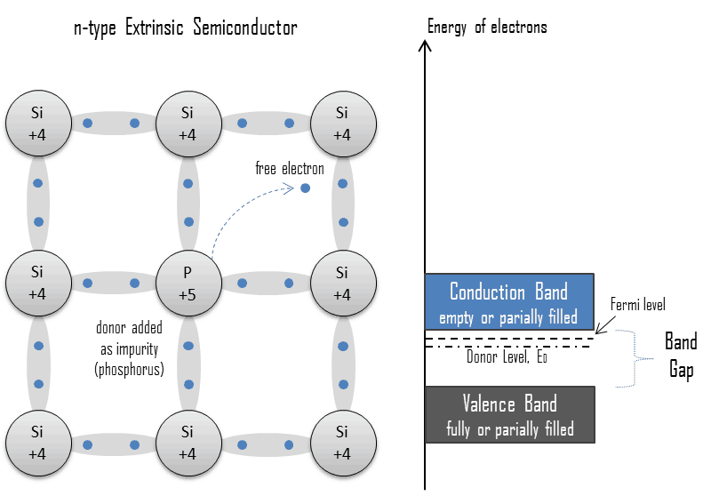
An extrinsic semiconductor which has been doped with electron donor atoms is called an n-type semiconductor, because the majority of charge carriers in the crystal are negative electrons. Since silicon is a tetravalent element, the normal crystal structure contains 4 covalent bonds from four valence electrons. In silicon, the most common dopants are group III and group V elements. Group V elements (pentavalent) have five valence electrons, which allows them to act as a donor. That means, the addition of these pentavalent impurities such as arsenic, antimony or phosphorus contributes free electrons, greatly increasing the conductivity of the intrinsic semiconductor. For example, a silicon crystal doped with boron (group III) creates a p-type semiconductor whereas a crystal doped with phosphorus (group V) results in an n-type semiconductor.
The conduction electrons are completely dominated by the number of donor electrons. Therefore:
The total number of conduction electrons is approximately equal to the number of donor sites, n≈ND.
Charge neutrality of semiconductor material is maintained because excited donor sites balance the conduction electrons. The net result is that the number of conduction electrons is increased, while the number of holes is reduced. The imbalance of the carrier concentration in the respective bands is expressed by the different absolute number of electrons and holes. Electrons are majority carriers, while holes are minority carriers in n-type material.
Donor Level
Donor Level
From the energy gap viewpoint, such impurities “create” energy levels in the band gap close to conduction band so that electrons can be easily excited from these levels into the conduction band. The electrons are said to be the “majority carriers” for current flow in an n-type semiconductor. This shifts the effective Fermi level to a point about halfway between the donor levels and the conduction band. Fermi level is the term used to describe the top of the collection of electron energy levels at absolute zero temperature. The Fermi level is the surface of Fermi sea at absolute zero where no electrons will have enough energy to rise above the surface. In pure semiconductors the position of the Fermi level is within the band gap, approximately in the middle of the band gap.
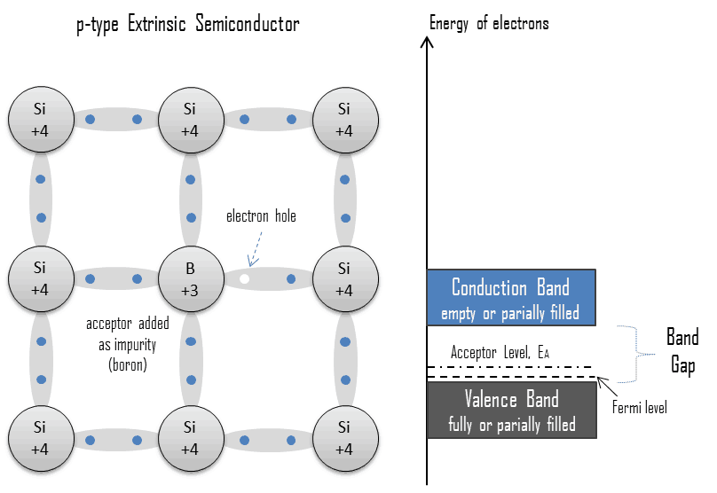
p-type Semiconductors
An extrinsic semiconductor which has been doped with electron acceptor atoms is called a p-type semiconductor, because the majority of charge carriers in the crystal are electron holes (positive charge carriers). The pure semiconductor silicon is a tetravalent element, the normal crystal structure contains 4 covalent bonds from four valence electrons. In silicon, the most common dopants are group III and group V elements. Group III elements (trivalent) all contain three valence electrons, causing them to function as acceptors when used to dope silicon. When an acceptor atom replaces a tetravalent silicon atom in the crystal, a vacant state (an electron hole) is created. An electron hole (often simply called a hole) is the lack of an electron at a position where one could exist in an atom or atomic lattice. It is one of the two types of charge carriers that are responsible for creating electric current in semiconducting materials. These positively charged holes can move from atom to atom in semiconducting materials as electrons leave their positions. The addition of trivalent impurities such as boron, aluminum or gallium to an intrinsic semiconductor creates these positive electron holes in the structure. For example, a silicon crystal doped with boron (group III) creates a p-type semiconductor whereas a crystal doped with phosphorus (group V) results in an n-type semiconductor.
The number of electron holes are completely dominated by the number of acceptor sites. Therefore:
The total number of holes is approximately equal to the number of donor sites, p ≈ NA.
Charge neutrality of this semiconductor material is also maintained. The net result is that the number of electron holes is increased, while the number of conduction electrons is reduced. The imbalance of the carrier concentration in the respective bands is expressed by the different absolute number of electrons and holes. Electron holes are majority carriers, while electrons are minority carriers in p-type material.
Acceptor Level
Acceptor Level
From the energy gap viewpoint, such impurities “create” energy levels within the band gap close to the valence band so that electrons can be easily excited from the valence band into these levels, leaving mobile holes in the valence band. They create “shallow” levels, levels that are very close to the valence band, so the energy required to ionize the atom (accept the electron that fills the hole and creates another hole further from the substituted atom) is small. This shifts the effective Fermi level to a point about halfway between the acceptor levels and the valence band. Fermi level is the term used to describe the top of the collection of electron energy levels at absolute zero temperature. The Fermi level is the surface of Fermi sea at absolute zero where no electrons will have enough energy to rise above the surface. In pure semiconductors the position of the Fermi level is within the band gap, approximately in the middle of the band gap.
The P-N Junction – Reverse Biased Junction
The semiconductor detector operates much better as a radiation detector if an external voltage is applied across the junction in the reverse biased direction. The depletion region will function as a radiation detector. Improvement can be reached by use of a reverse-bias voltage to the P-N junction to deplete the detector of free carriers, which is the principle of the most semiconductor detectors. Reverse biasing a junction increases the thickness of the depletion region because the potential difference across the junction is enhanced. Germanium detectors have a p-i-n structure in which the intrinsic (i) region is sensitive to ionizing radiation, particularly X rays and gamma rays. Under reverse bias, an electric field extends across the intrinsic or depleted region. In this case, negative voltage is applied to the p-side and positive to the second one. Holes in the p-region are attracted from the junction towards the p contact and similarly for electrons and the n contact. This charge, which is in proportion to the energy deposited in the detector by the incoming photon, is converted into a voltage pulse by an integral charge sensitive preamplifier.
See also: Germanium Detectors, MIRION Technologies. <available from: https://www.mirion.com/products/germanium-detectors>.
Robert Reed Burn, Introduction to Nuclear Reactor Operation, 1988.
U.S. Department of Energy, Nuclear Physics and Reactor Theory. DOE Fundamentals Handbook, Volume 1 and 2. January 1993.
Paul Reuss, Neutron Physics. EDP Sciences, 2008. ISBN: 978-2759800414.
See also:
Semiconductor Detectors
We hope, this article, Type of Semiconductors, helps you. If so, give us a like in the sidebar. Main purpose of this website is to help the public to learn some interesting and important information about radiation and dosimeters.
In solid-state physics, the valence band and conduction band are the bands closest to the Fermi level and thus determine the electrical conductivity of the semiconductor. Radiation Dosimetry
To understand the difference between metals, semiconductors and electrical insulators, we have to define the following terms from solid-state physics:
Valence Band
In solid-state physics, the valence band and conduction band are the bands closest to the Fermi level and thus determine the electrical conductivity of the solid. In electrical insulators and semiconductors, the valence band is the highest range of electron energies in which electrons are normally present at absolute zero temperature. For example, a silicon atom has fourteen electrons. In the ground state, they are arranged in the electron configuration [Ne]3s23p2. Of these, four are valence electrons, occupying the 3s orbital and two of the 3p orbitals. The distinction between the valence and conduction bands is meaningless in metals, because conduction occurs in one or more partially filled bands that take on the properties of both the valence and conduction bands.
Conduction Band
In solid-state physics, the valence band and conduction band are the bands closest to the Fermi level and thus determine the electrical conductivity of the solid. In electrical insulators and semiconductors, the conduction band is the lowest range of vacant electronic states. On a graph of the electronic band structure of a material, the valence band is located below the Fermi level, while the conduction band is located above it. In semiconductors, electrons may reach the conduction band, when they are excited, for example, by ionizing radiation (i.e. they must obtain energy higher than Egap). For example, diamond is a wide-band gap semiconductor (Egap = 5.47 eV) with high potential as an electronic device material in many devices. On the other side, germanium has a small band gap energy (Egap = 0.67 eV), which requires to operate the detector at cryogenic temperatures. The distinction between the valence and conduction bands is meaningless in metals, because conduction occurs in one or more partially filled bands that take on the properties of both the valence and conduction bands.
Robert Reed Burn, Introduction to Nuclear Reactor Operation, 1988.
U.S. Department of Energy, Nuclear Physics and Reactor Theory. DOE Fundamentals Handbook, Volume 1 and 2. January 1993.
Paul Reuss, Neutron Physics. EDP Sciences, 2008. ISBN: 978-2759800414.
See also:
Properties of Semiconductors
We hope, this article, Conduction and Valence Band in Semiconductors, helps you. If so, give us a like in the sidebar. Main purpose of this website is to help the public to learn some interesting and important information about radiation and dosimeters.
Semiconductivity is determined by the energy gap between valence and conduction bands. To understand, what is semiconductor, we have to define these terms. Radiation Dosimetry
In general, semiconductors are materials, inorganic or organic, which have the ability to control their conduction depending on chemical structure, temperature, illumination, and presence of dopants. The name semiconductor comes from the fact that these materials have an electrical conductivity between that of a metal, like copper, gold, etc. and an insulator, such as glass. They have an energy gap less than 4eV (about 1eV). In solid-state physics, this energy gap or band gap is an energy range between valence band and conduction band where electron states are forbidden. In contrast to conductors, electrons in a semiconductor must obtain energy (e.g. from ionizing radiation) to cross the band gap and to reach the conduction band. Properties of semiconductors are determined by the energy gap between valence and conduction bands. To understand, what is semiconductor, we have to define these terms.
Properties of Semiconductors
To understand the difference between metals, semiconductors and electrical insulators, we have to define the following terms from solid-state physics:
Valence Band. In solid-state physics, the valence band and conduction band are the bands closest to the Fermi level and thus determine the electrical conductivity of the solid. In electrical insulators and semiconductors, the valence band is the highest range of electron energies in which electrons are normally present at absolute zero temperature. For example, a silicon atom has fourteen electrons. In the ground state, they are arranged in the electron configuration [Ne]3s23p2. Of these, four are valence electrons, occupying the 3s orbital and two of the 3p orbitals. The distinction between the valence and conduction bands is meaningless in metals, because conduction occurs in one or more partially filled bands that take on the properties of both the valence and conduction bands.
Conduction Band. In solid-state physics, the valence band and conduction band are the bands closest to the Fermi level and thus determine the electrical conductivity of the solid. In electrical insulators and semiconductors, the conduction band is the lowest range of vacant electronic states. On a graph of the electronic band structure of a material, the valence band is located below the Fermi level, while the conduction band is located above it. In semiconductors, electrons may reach the conduction band, when they are excited, for example, by ionizing radiation (i.e. they must obtain energy higher than Egap). For example, diamond is a wide-band gap semiconductor (Egap = 5.47 eV) with high potential as an electronic device material in many devices. On the other side, germanium has a small band gap energy (Egap = 0.67 eV), which requires to operate the detector at cryogenic temperatures. The distinction between the valence and conduction bands is meaningless in metals, because conduction occurs in one or more partially filled bands that take on the properties of both the valence and conduction bands.
Band Gap. In solid-state physics, the energy gap or the band gap is an energy range between valence band and conduction band where electron states are forbidden. In contrast to conductors, electrons in a semiconductor must obtain energy (e.g. from ionizing radiation) to cross the band gap and to reach the conduction band. Band gaps are naturally different for different materials. For example, diamond is a wide-band gap semiconductor (Egap = 5.47 eV) with high potential as an electronic device material in many devices. On the other side, germanium has a small band gap energy (Egap = 0.67 eV), which requires to operate the detector at cryogenic temperatures.
Fermi Level. The term “Fermi level” comes from Fermi-Dirac statistics, which describes a distribution of particles over energy states in systems consisting of fermions (electrons) that obey the Pauli exclusion principle. Since they cannot exist in identical energy states, Fermi level is the term used to describe the top of the collection of electron energy levels at absolute zero temperature. The Fermi level is the surface of Fermi sea at absolute zero where no electrons will have enough energy to rise above the surface. In metals, the Fermi level lies in the hypothetical conduction band giving rise to free conduction electrons. In semiconductors the position of the Fermi level is within the band gap, approximately in the middle of the band gap.
Electron-hole Pair. In the semiconductor, free charge carriers are electrons and electron holes (electron-hole pairs). Electrons and holes are created by excitation of electron from valence band to the conduction band. An electron hole (often simply called a hole) is the lack of an electron at a position where one could exist in an atom or atomic lattice. It is one of the two types of charge carriers that are responsible for creating electric current in semiconducting materials. Since in a normal atom or crystal lattice the negative charge of the electrons is balanced by the positive charge of the atomic nuclei, the absence of an electron leaves a net positive charge at the hole’s location. Positively charged holes can move from atom to atom in semiconducting materials as electrons leave their positions. When an electron meets with a hole, they recombine and these free carriers effectively vanish. The recombination means an electron which has been excited from the valence band to the conduction band falls back to the empty state in the valence band, known as the holes.
The conductivity of a semiconductor can be modeled in terms of the band theory of solids. The band model of a semiconductor suggests that at ordinary temperatures there is a finite possibility that electrons can reach the conduction band and contribute to electrical conduction. In the semiconductor, free charge carriers (electron-hole pairs) are created by excitation of electron from valence band to the conduction band. This excitation left a hole in the valence band which behaves as positive charge and an electron-hole pair is created. Holes can sometimes be confusing as they are not physical particles in the way that electrons are, rather they are the absence of an electron in an atom. Holes can move from atom to atom in semiconducting materials as electrons leave their positions.
Robert Reed Burn, Introduction to Nuclear Reactor Operation, 1988.
U.S. Department of Energy, Nuclear Physics and Reactor Theory. DOE Fundamentals Handbook, Volume 1 and 2. January 1993.
Paul Reuss, Neutron Physics. EDP Sciences, 2008. ISBN: 978-2759800414.
See also:
Properties of Semiconductors
We hope, this article, Semiconductivity – Band Theory, helps you. If so, give us a like in the sidebar. Main purpose of this website is to help the public to learn some interesting and important information about radiation and dosimeters.
The basic principle of operation of scintillation counter involves the radiation reacting with a scintillator, which produces a series of flashes of varying intensity. Scintillation Counter – Principle of Operation – Description
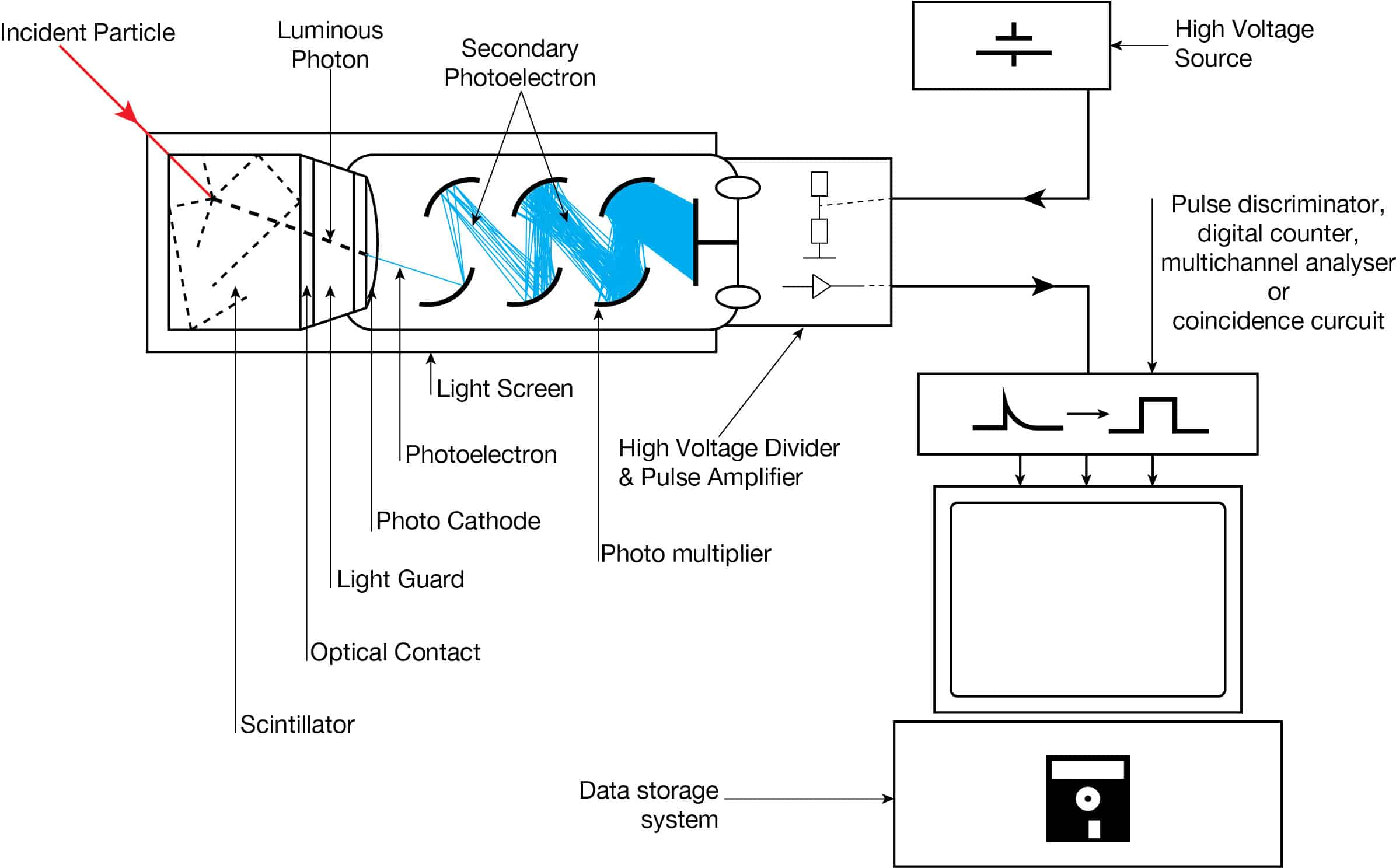
Apparatus with a scintillating crystal, photomultiplier, and data acquisition components. Source: wikipedia.org License CC BY-SA 3.0
A scintillation counter or scintillation detector is a radiation detector which uses the effect known as scintillation. Scintillation is a flash of light produced in a transparent material by the passage of a particle (an electron, an alpha particle, an ion, or a high-energy photon). Scintillation occurs in the scintillator, which is a key part of a scintillation detector. In general, a scintillation detector consists of:
Scintillator. A scintillator generates photons in response to incident radiation.
Photodetector. A sensitive photodetector (usually a photomultiplier tube (PMT), a charge-coupled device (CCD) camera, or a photodiode), which converts the light to an electrical signal and electronics to process this signal.
The basic principle of operation involves the radiation reacting with a scintillator, which produces a series of flashes of varying intensity. The intensity of the flashes is proportional to the energy of the radiation. This feature is very important. These counters are suited to measure the energy of gamma radiation (gamma spectroscopy) and, therefore, can be used to identify gamma emitting isotopes.
Scintillation Counter – Principle of Operation
The operation of scintillation counters is summarized in the following points:
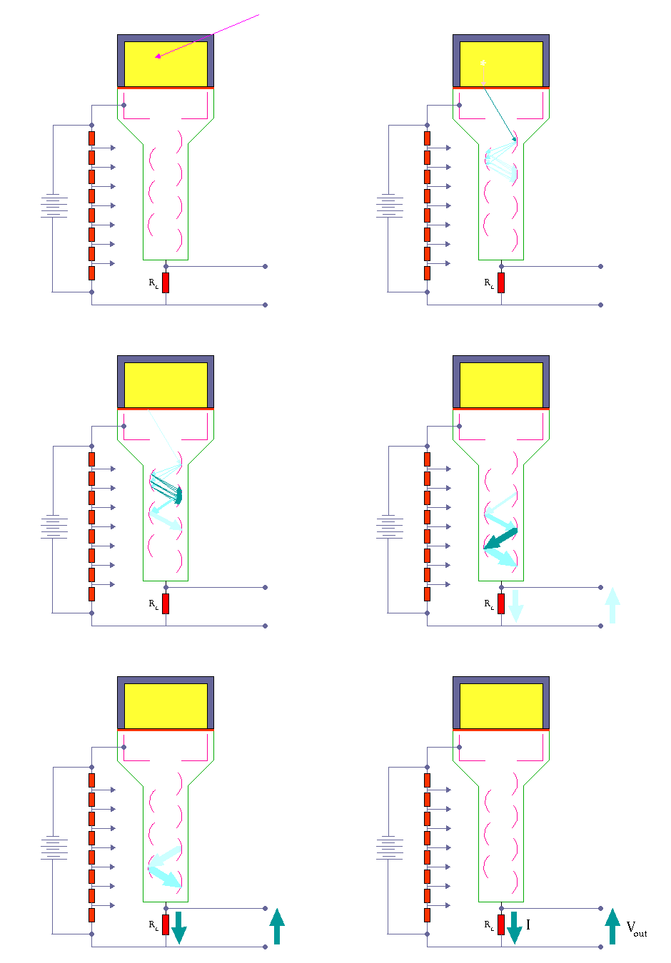
Scintillation Counter – Principle of Operation. Source: wikipedia.org License: Public Domain
Ionizing radiation enters the scintillator and interacts with the scintillator material. This cause electrons to be raised to an excited state.
For charged particles the track is the path of the particle itself.
The excited atoms of the scintillator material de-excite and rapidly emit a photon in the visible (or near-visible) light range. The quantity is proportional to the energy deposited by the ionizing particle. The material is said to fluoresce.
Three classes of phosphors are used:
inorganic crystals,
organic crystals,
plastic phosphors.
The light created in the scintillator strikes the photocathode of a photomultiplier tube, releasing at most one photoelectron per photon.
Using a voltage potential, this group of primary electrons is electrostatically accelerated and focused so that they strike the first dynode with enough energy to release additional electrons.
These secondary electrons are attracted and strike a second dynode releasing more electrons. This process occurs in the photomultiplier tube.
Each subsequent dynode impact releases further electrons, and so there is a current amplifying effect at each dynode stage. Each stage is at a higher potential than the previous to provide the accelerating field.
Primary signal is multiplied and this amplification continues through 10 to 12 stages.
At the final dynode, sufficient electrons are available to produce a pulse of sufficient magnitude for further amplification. This pulse carries information about the energy of the original incident radiation. The number of such pulses per unit time also gives information about the intensity of the radiation.
Robert Reed Burn, Introduction to Nuclear Reactor Operation, 1988.
U.S. Department of Energy, Nuclear Physics and Reactor Theory. DOE Fundamentals Handbook, Volume 1 and 2. January 1993.
Paul Reuss, Neutron Physics. EDP Sciences, 2008. ISBN: 978-2759800414.
See also:
Scintillation Counters
We hope, this article, Scintillation Counter – Principle of Operation, helps you. If so, give us a like in the sidebar. Main purpose of this website is to help the public to learn some interesting and important information about radiation and dosimeters.
Inorganic scintillators are usually crystals grown in high temperature furnaces. They include lithium iodide (LiI), sodium iodide (NaI), cesium iodide (CsI), and zinc sulfide (ZnS). Radiation Dosimetry
Scintillators are kinds of materials that provide detectable photons in the visible part of the light spectrum, following the passage of a charged particle or a photon. The scintillator consists of a transparent crystal, usually a phosphor, plastic or organic liquid that fluoresces when struck by ionizing radiation. The scintillator must also be transparent to its own light emissions and it must have a short decay time. The scintillator must be also shielded from all ambient light so that external photons do not swamp the ionization events caused by incident radiation. To achieve this a thin opaque foil, such as aluminized mylar, is often used, though it must have a low enough mass to minimize undue attenuation of the incident radiation being measured.
There are primarily two types of scintillators in common use in nuclear and particle physics: organic or plastic scintillators and inorganic or crystalline scintillators.
Inorganic Scintillators
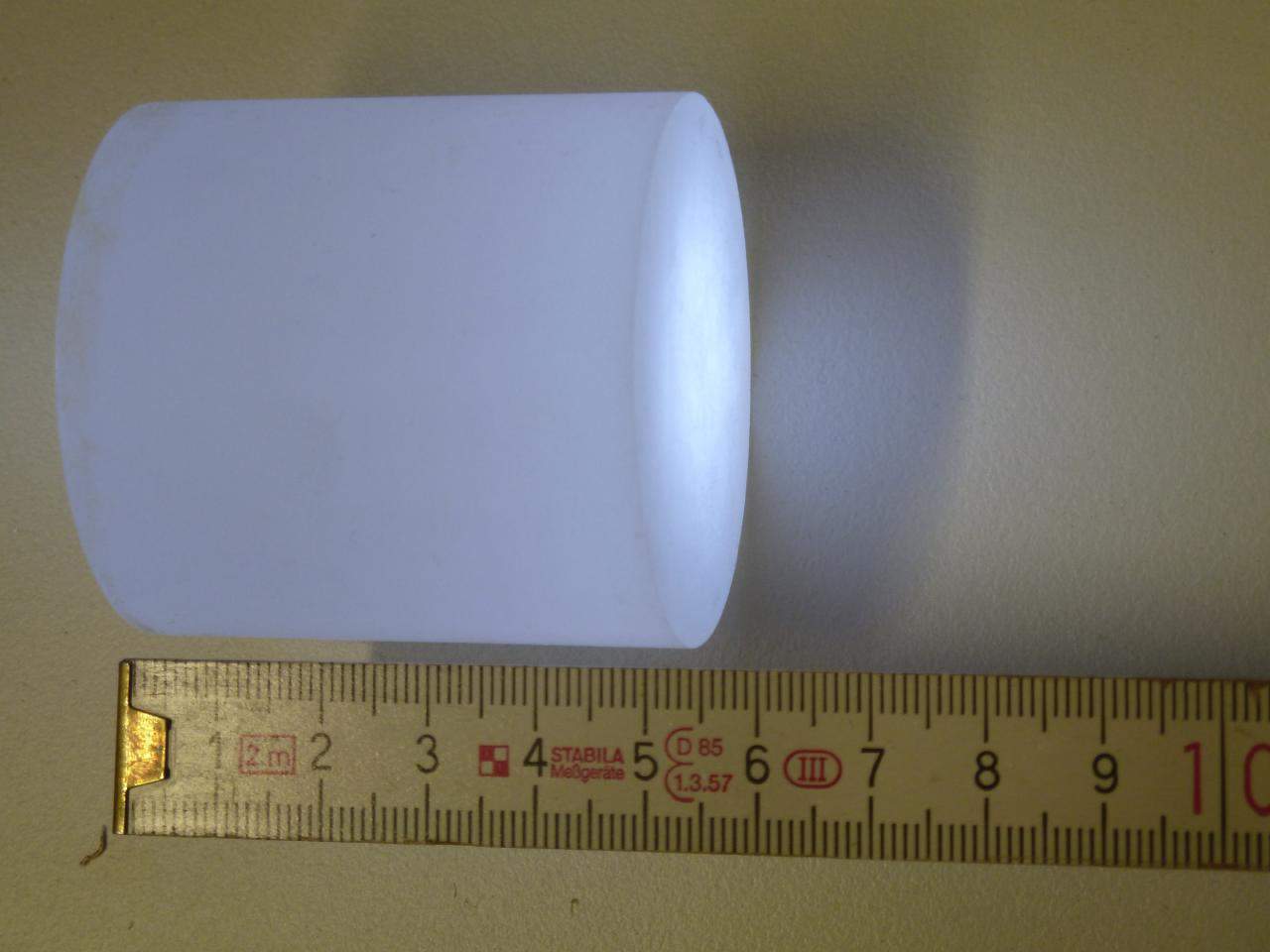
CsI(Tl) scintillation crystal. Source: wikipedia.de License: CC BY-SA 3.0
Inorganic scintillators are usually crystals grown in high temperature furnaces. They include lithium iodide (LiI), sodium iodide (NaI), cesium iodide (CsI), and zinc sulfide (ZnS). The most widely used scintillation material is NaI(Tl) (thallium-doped sodium iodide). The iodine provides most of the stopping power in sodium iodide (since it has a high Z = 53). These crystalline scintillators are characterized by high density, high atomic number, and pulse decay times of approximately 1 microsecond (~ 10-6 sec). Scintillation in inorganic crystals is typically slower than in organic ones. They exhibit high efficiency for detection of gamma rays and are capable of handling high count rates. Inorganic crystals can be cut to small sizes and arranged in an array configuration so as to provide position sensitivity. This feature is widely used in medical imaging to detect X-rays or gamma rays. Inorganic scintillators are better at detecting gamma rays and X-rays than organic scintillators. This is due to their high density and atomic number which gives a high electron density. A disadvantage of some inorganic crystals, e.g., NaI, is their hygroscopicity, a property which requires them to be housed in an airtight container to protect them from moisture.
Apparatus with a scintillating crystal, photomultiplier, and data acquisition components. Source: wikipedia.org License CC BY-SA 3.0
The most widely used scintillation material is NaI(Tl) (thallium-doped sodium iodide). NaI(Tl) as the scintillator is used in scintillation detectors, traditionally in nuclear medicine, geophysics, nuclear physics, and environmental measurements. The iodine provides most of the stopping power in sodium iodide (since it has a high Z = 53). These crystalline scintillators are characterized by high density, high atomic number, and pulse decay times of approximately 1 microsecond (~ 10-6 sec). The wavelength of maximum emission is 415 nm. Scintillation in inorganic crystals is typically slower than in organic ones. They exhibit high efficiency for detection of gamma rays and are capable of handling high count rates. Inorganic crystals can be cut to small sizes and arranged in an array configuration so as to provide position sensitivity. This feature is widely used in medical imaging to detect X-rays or gamma rays. Inorganic scintillators are better at detecting gamma rays and X-rays. This is due to their high density and atomic number which gives a high electron density. A disadvantage of some inorganic crystals, e.g., NaI, is their hygroscopicity, a property which requires them to be housed in an airtight container to protect them from moisture. The crystals are usually coupled with a photomultiplier tube, in a hermetically sealed assembly.
Caesium iodide (CsI) in crystalline form is used as the scintillator for the detection of protons and alpha particles. Pure CsI is a fast and dense scintillating material with relatively low light yield that increases significantly with cooling. The drawbacks of CsI are a high temperature gradient and a slight hygroscopicity.
Thallium-doped Caesium Iodide has an effective atomic number of 54 and a density of 4.51 g/cm3. CsI(TI) is also hygroscopic and should not be subjected to high humidity or water. CsI(TI) has different decay times for different particles (680ns and 3340ns) and can be used to determine between different kinds of radiation. The emission spectrum is peaked at 540-560 nm.
Robert Reed Burn, Introduction to Nuclear Reactor Operation, 1988.
U.S. Department of Energy, Nuclear Physics and Reactor Theory. DOE Fundamentals Handbook, Volume 1 and 2. January 1993.
Paul Reuss, Neutron Physics. EDP Sciences, 2008. ISBN: 978-2759800414.
See also:
Scintillation Counters
We hope, this article, Inorganic Scintillator – Scintillation Crystals, helps you. If so, give us a like in the sidebar. Main purpose of this website is to help the public to learn some interesting and important information about radiation and dosimeters.