In general, semiconductors are materials, inorganic or organic, which have the ability to control their conduction depending on chemical structure, temperature, illumination, and presence of dopants. The name semiconductor comes from the fact that these materials have an electrical conductivity between that of a metal, like copper, gold, etc. and an insulator, such as glass. They have an energy gap less than 4eV (about 1eV). In solid-state physics, this energy gap or band gap is an energy range between valence band and conduction band where electron states are forbidden. In contrast to conductors, electrons in a semiconductor must obtain energy (e.g. from ionizing radiation) to cross the band gap and to reach the conduction band. Properties of semiconductors are determined by the energy gap between valence and conduction bands. To understand, what is semiconductor, we have to define these terms.
Properties of Semiconductors
To understand the difference between metals, semiconductors and electrical insulators, we have to define the following terms from solid-state physics:
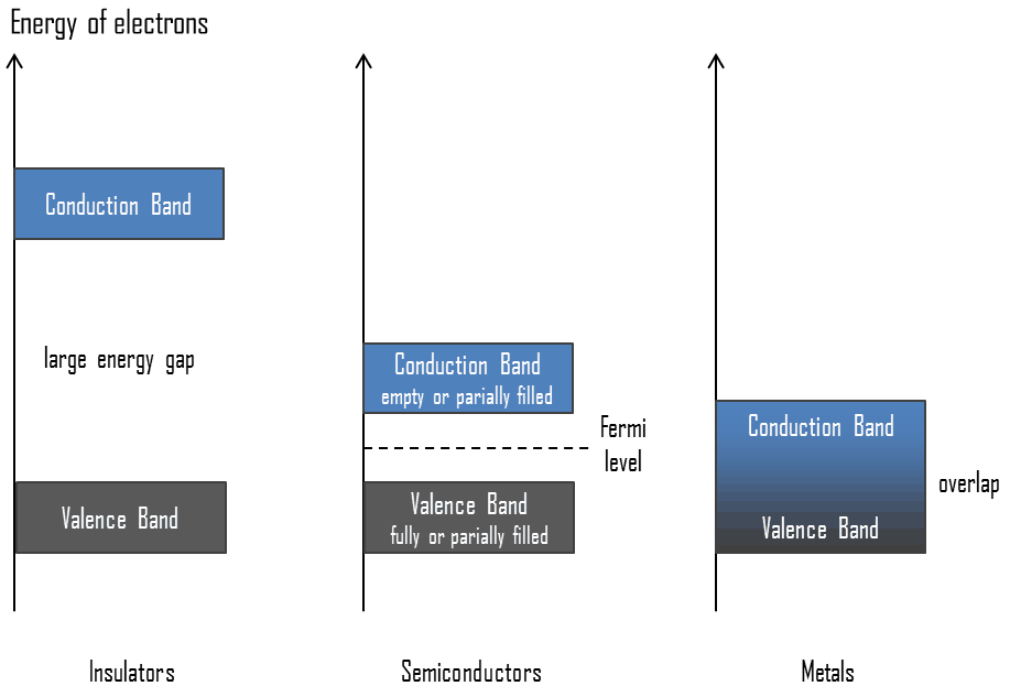 Valence Band. In solid-state physics, the valence band and conduction band are the bands closest to the Fermi level and thus determine the electrical conductivity of the solid. In electrical insulators and semiconductors, the valence band is the highest range of electron energies in which electrons are normally present at absolute zero temperature. For example, a silicon atom has fourteen electrons. In the ground state, they are arranged in the electron configuration [Ne]3s23p2. Of these, four are valence electrons, occupying the 3s orbital and two of the 3p orbitals. The distinction between the valence and conduction bands is meaningless in metals, because conduction occurs in one or more partially filled bands that take on the properties of both the valence and conduction bands.
- Conduction Band. In solid-state physics, the valence band and conduction band are the bands closest to the Fermi level and thus determine the electrical conductivity of the solid. In electrical insulators and semiconductors, the conduction band is the lowest range of vacant electronic states. On a graph of the electronic band structure of a material, the valence band is located below the Fermi level, while the conduction band is located above it. In semiconductors, electrons may reach the conduction band, when they are excited, for example, by ionizing radiation (i.e. they must obtain energy higher than Egap). For example, diamond is a wide-band gap semiconductor (Egap = 5.47 eV) with high potential as an electronic device material in many devices. On the other side, germanium has a small band gap energy (Egap = 0.67 eV), which requires to operate the detector at cryogenic temperatures. The distinction between the valence and conduction bands is meaningless in metals, because conduction occurs in one or more partially filled bands that take on the properties of both the valence and conduction bands.
- Band Gap. In solid-state physics, the energy gap or the band gap is an energy range between valence band and conduction band where electron states are forbidden. In contrast to conductors, electrons in a semiconductor must obtain energy (e.g. from ionizing radiation) to cross the band gap and to reach the conduction band. Band gaps are naturally different for different materials. For example, diamond is a wide-band gap semiconductor (Egap = 5.47 eV) with high potential as an electronic device material in many devices. On the other side, germanium has a small band gap energy (Egap = 0.67 eV), which requires to operate the detector at cryogenic temperatures.
- Fermi Level. The term “Fermi level” comes from Fermi-Dirac statistics, which describes a distribution of particles over energy states in systems consisting of fermions (electrons) that obey the Pauli exclusion principle. Since they cannot exist in identical energy states, Fermi level is the term used to describe the top of the collection of electron energy levels at absolute zero temperature. The Fermi level is the surface of Fermi sea at absolute zero where no electrons will have enough energy to rise above the surface. In metals, the Fermi level lies in the hypothetical conduction band giving rise to free conduction electrons. In semiconductors the position of the Fermi level is within the band gap, approximately in the middle of the band gap.
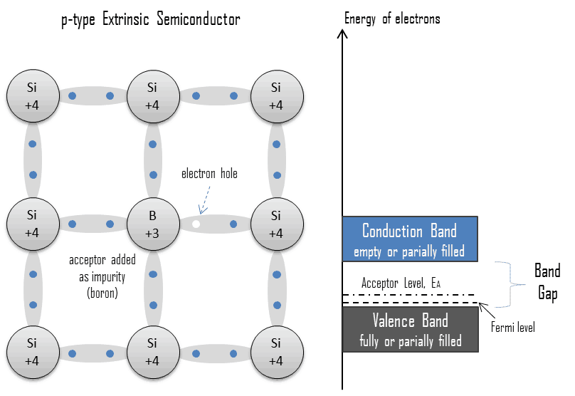 Electron-hole Pair. In the semiconductor, free charge carriers are electrons and electron holes (electron-hole pairs). Electrons and holes are created by excitation of electron from valence band to the conduction band. An electron hole (often simply called a hole) is the lack of an electron at a position where one could exist in an atom or atomic lattice. It is one of the two types of charge carriers that are responsible for creating electric current in semiconducting materials. Since in a normal atom or crystal lattice the negative charge of the electrons is balanced by the positive charge of the atomic nuclei, the absence of an electron leaves a net positive charge at the hole’s location. Positively charged holes can move from atom to atom in semiconducting materials as electrons leave their positions. When an electron meets with a hole, they recombine and these free carriers effectively vanish. The recombination means an electron which has been excited from the valence band to the conduction band falls back to the empty state in the valence band, known as the holes.
The conductivity of a semiconductor can be modeled in terms of the band theory of solids. The band model of a semiconductor suggests that at ordinary temperatures there is a finite possibility that electrons can reach the conduction band and contribute to electrical conduction. In the semiconductor, free charge carriers (electron-hole pairs) are created by excitation of electron from valence band to the conduction band. This excitation left a hole in the valence band which behaves as positive charge and an electron-hole pair is created. Holes can sometimes be confusing as they are not physical particles in the way that electrons are, rather they are the absence of an electron in an atom. Holes can move from atom to atom in semiconducting materials as electrons leave their positions.
Electron Excitation in Semiconductors
Energy for the excitation can be obtained by different ways.
Thermal Excitation
Electron-hole pairs are constantly generated from thermal energy as well, in the absence of any external energy source. Thermal excitation does not require any other form of starting impulse. This phenomenon occurs also at room temperature. It is caused by impurities, irregularity in structure lattice or by dopant. It strongly depends on the Egap (a distance between valence and conduction band), so that for lower Egap a number of thermally excited charge carriers increases. Since thermal excitation results in the detector noise, active cooling is required for some types of semiconductors (e.g. germanium). Detectors based on silicon have sufficiently low noise even by room temperature. This is caused by the large band gap of silicon (Egap= 1.12 eV), which allows us to operate the detector at room temperature, but cooling is prefered to reduce noise.
Optical Excitation
Note that, energy of a single photon of visible light spectrum is comparable with these band gaps. Photons of wave lengths 700 nm – 400 nm have energies of 1.77 eV 3.10 eV. As a result, also visible light is able to excite electrons to the conduction band. Actually, this is the principle of photovoltaic panels that generate electric current.
Excitation by Ionizing Radiation
Electrons may reach the conduction band, when they are excited by ionizing radiation (i.e. they must obtain energy higher than Egap). In general, heavy charged particles transfer energy mostly by:
- Excitation. The charged particle can transfer energy to the atom, raising electrons to a higher energy levels.
- Ionization. Ionization can occur, when the charged particle have enough energy to remove an electron. This results in a creation of ion pairs in surrounding matter.
A convenient variable that describes the ionization properties of surrounding medium is the stopping power. The classical expression that describes the specific energy loss is known as the Bethe formula. For alpha particles and heavier particles the stopping power of most materials is very high for heavy charged particles and these particles have very short ranges.
In addition to these interactions, beta particles also lose energy by radiative process known as the bremsstrahlung. From classical theory, when a charged particle is accelerated or decelerated, it must radiate energy and the deceleration radiation is known as the bremsstrahlung (“braking radiation”).
Photons (gamma rays and X-rays) can ionize atoms directly (despite they are electrically neutral) through the Photoelectric effect and the Compton effect, but secondary (indirect) ionization is much more significant. Although a large number of possible interactions are known, there are three key interaction mechanisms with matter.
In all cases, a particle of ionizing radiation deposits a portion of its energy along its path. Particle passing through the detector ionizes the atoms of semiconductor, producing the electron-hole pairs. For example, typical thickness of silicon detector is about 300 µm so the number of generated electron-hole pairs by minimum ionizing particle (MIP) passing perpendicular through the detector is about 3.2 x 10⁴. This value is minor in comparison the total number of free carriers in intrinsic semiconductor of a surface of 1 cm2 and the same thickness. Note that, a sample of pure germanium at 20 °C contains about 1.26×10²¹ atoms, but also contains 7.5 x 10¹¹ free electrons and 7.5 x 10¹¹ holes constantly generated from thermal energy. As can be seen, the signal to noise ratio (S/N) would be minimal. The addition of 0.001% of arsenic (an impurity) donates an extra 1015 free electrons in the same volume and the electrical conductivity is increased by a factor of 10,000. In doped material the signal to noise ratio (S/N) would be even smaller. Cooling of the semiconductor is one way to lower this ratio.
Improvement can be reached by use of a reverse-bias voltage to the P-N junction to deplete the detector of free carriers, which is the principle of the most silicon radiation detectors. In this case, negative voltage is applied to the p-side and positive to the second one. Holes in the p-region are attracted from the junction towards the p contact and similarly for electrons and the n contact.
We hope, this article, Semiconductor – Properties of Semiconductors, helps you. If so, give us a like in the sidebar. Main purpose of this website is to help the public to learn some interesting and important information about radiation and dosimeters.