Facebook Instagram Youtube Twitter

What is Dopant in Semiconductors – Definition

In general, there are two types of dopant atoms resulting in two types of extrinsic semiconductors. The most common dopants are group III and group V elements

A doped semiconductor, is a semiconductor, that was intentionally doped for the purpose of modulating its electrical, optical and structural properties. In case of semiconductor detectors of ionizing radiation, doping is the intentional introduction of impurities into an intrinsic semiconductor for the purpose of changes in their electrical properties. Therefore, intrinsic semiconductors are also known as pure semiconductors or i-type semiconductors.

The addition of a small percentage of foreign atoms in the regular crystal lattice of silicon or germanium produces dramatic changes in their electrical properties, since these foreign atoms incorporated into the crystal structure of the semiconductor provide free charge carriers (electrons or electron holes) in the semiconductor. In an extrinsic semiconductor it is these foreign dopant atoms in the crystal lattice that mainly provide the charge carriers which carry electric current through the crystal. In general, there are two types of dopant atoms resulting in two types of extrinsic semiconductors. These dopants that produce the desired controlled changes are classified as either electron acceptors or donors and the corresponding doped semiconductors are known as:

  • n-type Semiconductors.
  • p-type Semiconductors.

Extrinsic semiconductors are components of many common electrical devices, as well of many detectors of ionizing radiation. For these purpose, a semiconductor diode (devices that allow current in only one direction) usually consists of p-type and n-type semiconductors placed in junction with one another.

Electron Donor – Group V Dopant
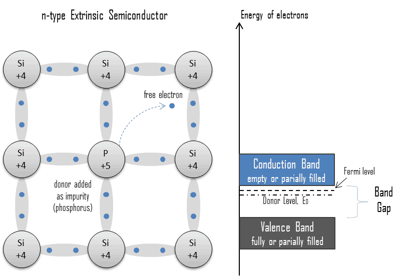
extrinsic - doped semiconductor - n-type - donorAn extrinsic semiconductor which has been doped with electron donor atoms is called an n-type semiconductor, because the majority of charge carriers in the crystal are negative electrons. Since silicon is a tetravalent element, the normal crystal structure contains 4 covalent bonds from four valence electrons. In silicon, the most common dopants are group III and group V elements. Group V elements (pentavalent) have five valence electrons, which allows them to act as a donor. That means, the addition of these pentavalent impurities such as arsenic, antimony or phosphorus contributes free electrons, greatly increasing the conductivity of the intrinsic semiconductor. For example, a silicon crystal doped with boron (group III) creates a p-type semiconductor whereas a crystal doped with phosphorus (group V) results in an n-type semiconductor.

The conduction electrons are completely dominated by the number of donor electrons. Therefore:

The total number of conduction electrons is approximately equal to the number of donor sites, n≈ND.

Charge neutrality of semiconductor material is maintained because excited donor sites balance the conduction electrons. The net result is that the number of conduction electrons is increased, while the number of holes is reduced. The imbalance of the carrier concentration in the respective bands is expressed by the different absolute number of electrons and holes. Electrons are majority carriers, while holes are minority carriers in n-type material.

Electron Acceptor – Group III Dopant
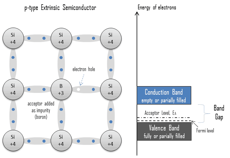
extrinsic - doped semiconductor - p-type - acceptorAn extrinsic semiconductor which has been doped with electron acceptor atoms is called a p-type semiconductor, because the majority of charge carriers in the crystal are electron holes (positive charge carriers). The pure semiconductor silicon is a tetravalent element, the normal crystal structure contains 4 covalent bonds from four valence electrons. In silicon, the most common dopants are group III and group V elements. Group III elements (trivalent) all contain three valence electrons, causing them to function as acceptors when used to dope silicon. When an acceptor atom replaces a tetravalent silicon atom in the crystal, a vacant state (an electron hole) is created. An electron hole (often simply called a hole) is the lack of an electron at a position where one could exist in an atom or atomic lattice. It is one of the two types of charge carriers that are responsible for creating electric current in semiconducting materials. These positively charged holes can move from atom to atom in semiconducting materials as electrons leave their positions. The addition of trivalent impurities such as boron, aluminum or gallium to an intrinsic semiconductor creates these positive electron holes in the structure. For example, a silicon crystal doped with boron (group III) creates a p-type semiconductor whereas a crystal doped with phosphorus (group V) results in an n-type semiconductor.

The number of electron holes are completely dominated by the number of acceptor sites. Therefore:

The total number of holes is approximately equal to the number of donor sites, p ≈ NA.

Charge neutrality of this semiconductor material is also maintained. The net result is that the number of electron holes is increased, while the number of conduction electrons is reduced. The imbalance of the carrier concentration in the respective bands is expressed by the different absolute number of electrons and holes. Electron holes are majority carriers, while electrons are minority carriers in p-type material.

References:

Radiation Protection:

  1. Knoll, Glenn F., Radiation Detection and Measurement 4th Edition, Wiley, 8/2010. ISBN-13: 978-0470131480.
  2. Stabin, Michael G., Radiation Protection and Dosimetry: An Introduction to Health Physics, Springer, 10/2010. ISBN-13: 978-1441923912.
  3. Martin, James E., Physics for Radiation Protection 3rd Edition, Wiley-VCH, 4/2013. ISBN-13: 978-3527411764.
  4. U.S.NRC, NUCLEAR REACTOR CONCEPTS
  5. U.S. Department of Energy, Instrumantation and Control. DOE Fundamentals Handbook, Volume 2 of 2. June 1992.

Nuclear and Reactor Physics:

  1. J. R. Lamarsh, Introduction to Nuclear Reactor Theory, 2nd ed., Addison-Wesley, Reading, MA (1983).
  2. J. R. Lamarsh, A. J. Baratta, Introduction to Nuclear Engineering, 3d ed., Prentice-Hall, 2001, ISBN: 0-201-82498-1.
  3. W. M. Stacey, Nuclear Reactor Physics, John Wiley & Sons, 2001, ISBN: 0- 471-39127-1.
  4. Glasstone, Sesonske. Nuclear Reactor Engineering: Reactor Systems Engineering, Springer; 4th edition, 1994, ISBN: 978-0412985317
  5. W.S.C. Williams. Nuclear and Particle Physics. Clarendon Press; 1 edition, 1991, ISBN: 978-0198520467
  6. G.R.Keepin. Physics of Nuclear Kinetics. Addison-Wesley Pub. Co; 1st edition, 1965
  7. Robert Reed Burn, Introduction to Nuclear Reactor Operation, 1988.
  8. U.S. Department of Energy, Nuclear Physics and Reactor Theory. DOE Fundamentals Handbook, Volume 1 and 2. January 1993.
  9. Paul Reuss, Neutron Physics. EDP Sciences, 2008. ISBN: 978-2759800414.

See also:

Types of Semiconductors

We hope, this article, Dopant in Semiconductors, helps you. If so, give us a like in the sidebar. Main purpose of this website is to help the public to learn some interesting and important information about radiation and dosimeters.
What is Principle of Operation of Semiconductor Detectors – Definition

This article summarizes principle of operation of semiconductor detectors. Ionizing radiation enters the sensitive volume of the detector and interacts with the semiconductor material. Radiation Dosimetry
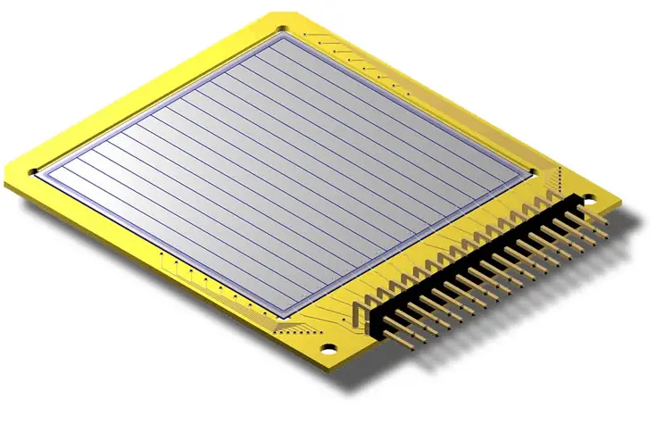
silicon strip detector - semiconductors
Silicin Strip Detector Source: micronsemiconductor.co.uk

A semiconductor detector is a radiation detector which is based on a semiconductor, such as silicon or germanium to measure the effect of incident charged particles or photons. In general, semiconductors are materials, inorganic or organic, which have the ability to control their conduction depending on chemical structure, temperature, illumination, and presence of dopants. The name semiconductor comes from the fact that these materials  have an electrical conductivity between that of a metal, like copper, gold, etc. and an insulator, such as glass. They have an energy gap less than 4eV (about 1eV). In solid-state physics, this energy gap or band gap is an energy range between valence band and conduction band where electron states are forbidden. In contrast to conductors, electrons in a semiconductor must obtain energy (e.g. from ionizing radiation) to cross the band gap and to reach the conduction band.

Principle of Operation of Semiconductor Detectors  

The operation of semiconductor detectors is  summarized in the following points:

  • Ionizing radiation enters the sensitive volume of the detector and interacts with the semiconductor material.
  • Particle passing through the detector ionizes the atoms of semiconductor, producing the electron-hole pairs. The number of electron-hole pairs is proportional to the energy of the radiation to the semiconductor. As a result, a number of electrons are transferred from the valence band to the conduction band, and an equal number of holes are created in the valence band.
  • Under the influence of an electric field, electrons and holes travel to the electrodes, where they result in a pulse that can be measured in an outer circuit,
  • This pulse carries information about the energy of the original incident radiation. The number of such pulses per unit time also gives information about the intensity of the radiation.

The energy required to produce electron-hole-pairs is very low compared to the energy required to produce paired ions in a gaseous ionization detector. In semiconductor detectors the statistical variation of the pulse height is smaller and the energy resolution is higher. As the electrons travel fast, the time resolution is also very good. Compared with gaseous ionization detectors, the density of a semiconductor detector is very high, and charged particles of high energy can give off their energy in a semiconductor of relatively small dimensions.

References:

Radiation Protection:

  1. Knoll, Glenn F., Radiation Detection and Measurement 4th Edition, Wiley, 8/2010. ISBN-13: 978-0470131480.
  2. Stabin, Michael G., Radiation Protection and Dosimetry: An Introduction to Health Physics, Springer, 10/2010. ISBN-13: 978-1441923912.
  3. Martin, James E., Physics for Radiation Protection 3rd Edition, Wiley-VCH, 4/2013. ISBN-13: 978-3527411764.
  4. U.S.NRC, NUCLEAR REACTOR CONCEPTS
  5. U.S. Department of Energy, Instrumantation and Control. DOE Fundamentals Handbook, Volume 2 of 2. June 1992.

Nuclear and Reactor Physics:

  1. J. R. Lamarsh, Introduction to Nuclear Reactor Theory, 2nd ed., Addison-Wesley, Reading, MA (1983).
  2. J. R. Lamarsh, A. J. Baratta, Introduction to Nuclear Engineering, 3d ed., Prentice-Hall, 2001, ISBN: 0-201-82498-1.
  3. W. M. Stacey, Nuclear Reactor Physics, John Wiley & Sons, 2001, ISBN: 0- 471-39127-1.
  4. Glasstone, Sesonske. Nuclear Reactor Engineering: Reactor Systems Engineering, Springer; 4th edition, 1994, ISBN: 978-0412985317
  5. W.S.C. Williams. Nuclear and Particle Physics. Clarendon Press; 1 edition, 1991, ISBN: 978-0198520467
  6. G.R.Keepin. Physics of Nuclear Kinetics. Addison-Wesley Pub. Co; 1st edition, 1965
  7. Robert Reed Burn, Introduction to Nuclear Reactor Operation, 1988.
  8. U.S. Department of Energy, Nuclear Physics and Reactor Theory. DOE Fundamentals Handbook, Volume 1 and 2. January 1993.
  9. Paul Reuss, Neutron Physics. EDP Sciences, 2008. ISBN: 978-2759800414.

See also:

Semiconductors

We hope, this article, Principle of Operation of Semiconductor Detectors, helps you. If so, give us a like in the sidebar. Main purpose of this website is to help the public to learn some interesting and important information about radiation and dosimeters.
What is Silicon-based Semiconductor Detector – Definition

Silicon-based semiconductor detectors are mainly used for charged particle detectors (especially for tracking charged particles) and soft X-ray detectors. Radiation Dosimetry
silicon strip detector - semiconductors
Silicin Strip Detector Source: micronsemiconductor.co.uk

Silicon-based semiconductor detectors are mainly used for charged particle detectors (especially for tracking charged particles) and soft X-ray detectors while germanium is widely used for gamma ray spectroscopy. A large, clean and almost perfect semiconductor is ideal as a counter for radioactivity. However, it is difficult to make large crystals with sufficient purity. The semiconductor detectors have, therefore, low efficiency, but they do give a very precise measure of the energy. Detectors based on silicon have sufficiently low noise even by room temperature. This is caused by the large band gap of silicon (Egap= 1.12 eV), which allows us to operate the detector at room temperature, but cooling is prefered to reduce noise. The drawback is that silicon detectors are much more expensive than cloud chambers or wire chambers and require sophisticated cooling to reduce leakage currents (noise). They also suffer degradation over time from radiation, however this can be greatly reduced thanks to the Lazarus effect.

Principle of Operation of Silicon Detectors  

The operation of semiconductor detectors is  summarized in the following points:

  • Ionizing radiation enters the sensitive volume of the detector and interacts with the semiconductor material.
  • Particle passing through the detector ionizes the atoms of semiconductor, producing the electron-hole pairs. The number of electron-hole pairs is proportional to the energy of the radiation to the semiconductor. As a result, a number of electrons are transferred from the valence band to the conduction band, and an equal number of holes are created in the valence band.
  • Under the influence of an electric field, electrons and holes travel to the electrodes, where they result in a pulse that can be measured in an outer circuit,
  • This pulse carries information about the energy of the original incident radiation. The number of such pulses per unit time also gives information about the intensity of the radiation.

The energy required to produce electron-hole-pairs is very low compared to the energy required to produce paired ions in a gaseous ionization detector. In semiconductor detectors the statistical variation of the pulse height is smaller and the energy resolution is higher. As the electrons travel fast, the time resolution is also very good. Compared with gaseous ionization detectors, the density of a semiconductor detector is very high, and charged particles of high energy can give off their energy in a semiconductor of relatively small dimensions.

Properties of Silicon

Properties of Silicon

There are many semiconductors in nature and others synthesized in laboratories; however, the best known are silicon (Si) and germanium (Ge). Silicon has the following properties:

  • silicon - semiconducting material
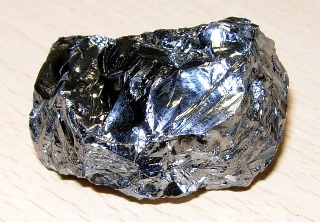
    Purified silicon. Source: wikipedia.org License: Public Domain

    Silicon. Silicon is a chemical element with atomic number 14 which means there are 14 protons and 14 electrons in the atomic structure. The chemical symbol for Silicon is Si. Silicon is a hard and brittle crystalline solid with a blue-grey metallic lustre, it is a tetravalent metalloid and semiconductor.

  • Silicon is mainly used for charged particle detectors (especially for tracking charged particles) and soft X-ray detectors. The large band-gap energy (Egap= 1.12 eV) allows us to operate the detector at room temperature, but cooling is prefered to reduce noise. Silicon based detectors are very important in high-energy physics. Since silicon-based detectors are very good for tracking charged particles, they constitute a substantial part of detection system at the LHC in CERN.
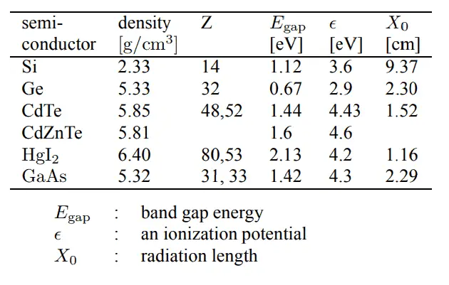
  • The average energy for creation of electron-hole pair is 3.6 eV. This value is approximately 10 times lower compared to the ionization energy of gases used in proportional chambers, drift chambers and etc. And it leads to massive creation of charge carriers.
  • Silicon has a high density of  2.329 g/cm3 and therefore the average energy loss per unit of length allows building thin detectors (e.g. 300 µm) that still produce measurable signals. For example, in case of minimum ionizing particle (MIP) the energy loss is 390 eV/µm.
  • semiconductor detectors - table of parametersThe silicon detectors are mechanically rigid and therefore no special supporting structures are needed.
  • High mobility of the charge carriers (electrons – 1450 cm2V−1 s −1 , holes – 450 cm2V−1 s −1) means rapid charge carriers collection (≪10 ns) and short dead time. Width of the readout pulse at half maximum (full width at half maximum – FWHM) is about 20 ns.
  • Silicon detectors can be used in strong magnetic fields.

In all cases, a particle of ionizing radiation deposits a portion of its energy along its path. Particle passing through the detector ionizes the atoms of semiconductor, producing the electron-hole pairs. For example, typical thickness of silicon detector is about 300 µm so the number of generated electron-hole pairs by minimum ionizing particle (MIP) passing perpendicular through the detector is about 3.2 x 10⁴. This value is minor in comparison the total number of free carriers in intrinsic semiconductor of a surface of 1 cm2 and the same thickness. Note that, a sample of pure germanium at 20 °C contains about 1.26×10²¹ atoms, but also contains 7.5 x 10¹¹ free electrons and 7.5 x 10¹¹ holes constantly generated from thermal energy. As can be seen, the signal to noise ratio (S/N) would be minimal. The addition of 0.001% of arsenic (an impurity) donates an extra 1015 free electrons in the same volume and the electrical conductivity is increased by a factor of 10,000. In doped material the signal to noise ratio (S/N) would be even smaller. Cooling of the semiconductor is one way to lower this ratio.

See also: Doped Semiconductor

Improvement can be reached by use of a reverse-bias voltage to the P-N junction to deplete the detector of free carriers, which is the principle of the most silicon radiation detectors. In this case, negative voltage is applied to the p-side and positive to the second one. Holes in the p-region are attracted from the junction towards the p contact and similarly for electrons and the n contact.

Application of Silicon Detectors

Since silicon-based detectors are very good for tracking charged particles, they constitute a substantial part of detection system at the LHC in CERN. Most silicon particle detectors work, in principle, by doping narrow (usually around 100 micrometers wide) strips of silicon to turn them into diodes, which are then reverse biased. As charged particles pass through these strips, they cause small ionization currents that can be detected and measured. Arranging thousands of these detectors around a collision point in a particle accelerator can yield an accurate picture of what paths particles take. For example, the Inner Tracking System (ITS) of a Large Ion Collider Experiment (ALICE) contains three layers of silicon-based detectors:

  • Silicon Pixel Detector (SPD)
  • Silicon Drift Detector (SDD)
  • Silicon Strip Detector (SSD)

Silicon Strip Detectors

Silicon-based detectors are very good for tracking charged particles. A silicon strip detector is an arrangement of strip like shaped implants acting as charge collecting electrodes.

Silicon strip detectors 5 x 5 cm2 in area are quite common and are used in series (just like planes of MWPCs) to determine charged-particle trajectories to position-accuracies of the order of several μm in the transverse direction.  Placed on a low doped fully depleted silicon wafer these implants form a one-dimensional array of diodes. By connecting each of the metalized strips to a charge sensitive amplifier a position sensitive detector is built. Two dimensional position measurements can be achieved by applying an additional strip like doping on the wafer backside by use of a double sided technology.  Such devices can be used to measure small impact parameters and thereby determine whether some charged particle originated from a primary collision or was the decay product of a primary particle that traveled a small distance from the original interaction, and then decayed.

Silicon strip detectors constitute a substantial part of detection system at the LHC in CERN. Most silicon particle detectors work, in principle, by doping narrow (usually around 100 micrometers wide) strips of silicon to turn them into diodes, which are then reverse biased. As charged particles pass through these strips, they cause small ionization currents that can be detected and measured. Arranging thousands of these detectors around a collision point in a particle accelerator can yield an accurate picture of what paths particles take.

For example, the Inner Tracking System (ITS) of a Large Ion Collider Experiment (ALICE) contains three layers of silicon-based detectors:

  • Silicon Pixel Detector (SPD)
  • Silicon Drift Detector (SDD)
  • Silicon Strip Detector (SSD)

Delta E – E Detector – Telescope

delta E - E Telescope - chart
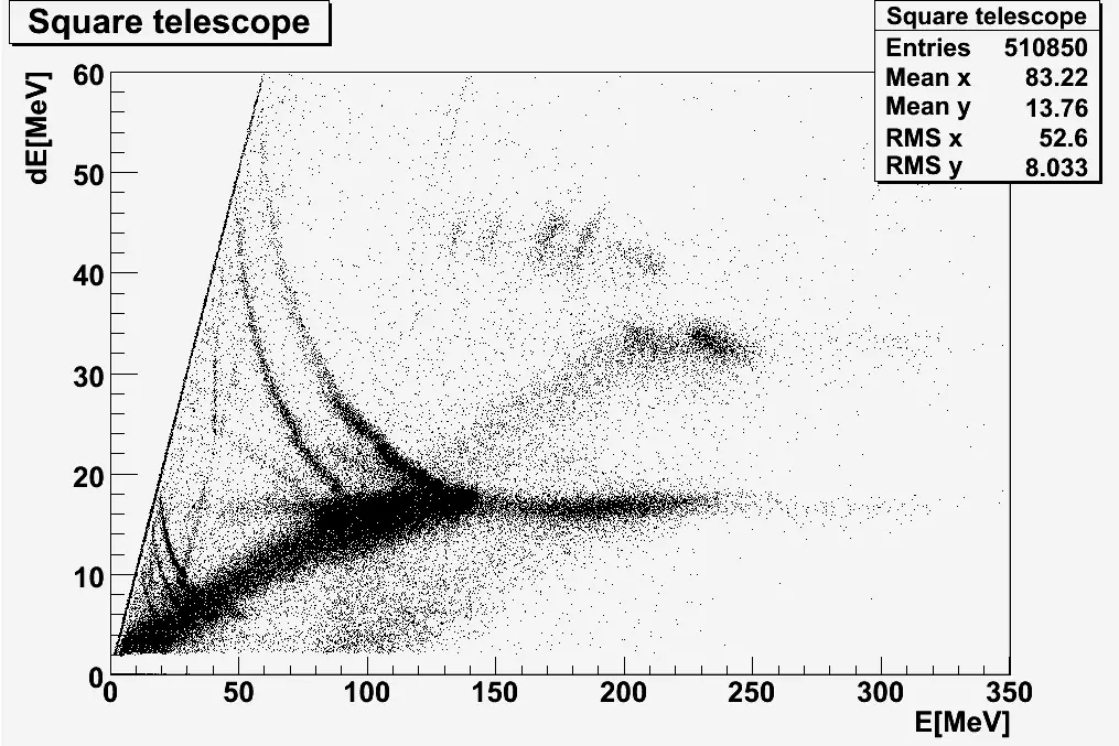
Example of histogram from ΔE-E detector. Each hyperbola-like curve represents different particle in the beam.

In experimental physics, ΔE-E detectors, known as telescopes, are powerful devices for charged particles identification. In order to provide charged-particle identification, telescopes consisting of pairs of thin and thick surface-barrier detectors can be used. These detectors must be positioned in series. The velocity is deduced from the stopping power measured in the thin detectors (ΔE detectors). There is a strong correlation between the energy deposited in each detector. This correlation depends on the mass (A), the charge (Z) and the kinetic energy (E) of each particle. The mass is deduced from the range or from the total kinetic energy loss in the thicker detector (E detector).

Telescopes can be  composed of several detectors (ionization chambers, silicon detectors and scintillators for instance) stacked in order to slow down incident charged particles, the first detector being the thinnest and the last one the thickest. CsI scintillation counters can be, for example used as final E counters. As an example of telescope, an assembly based on two front ΔE silicon detectors (10 or 30 µm) and an E silicon counter 1500 µm thick may be used for detection of high-energy charged particles.

References:

Radiation Protection:

  1. Knoll, Glenn F., Radiation Detection and Measurement 4th Edition, Wiley, 8/2010. ISBN-13: 978-0470131480.
  2. Stabin, Michael G., Radiation Protection and Dosimetry: An Introduction to Health Physics, Springer, 10/2010. ISBN-13: 978-1441923912.
  3. Martin, James E., Physics for Radiation Protection 3rd Edition, Wiley-VCH, 4/2013. ISBN-13: 978-3527411764.
  4. U.S.NRC, NUCLEAR REACTOR CONCEPTS
  5. U.S. Department of Energy, Instrumantation and Control. DOE Fundamentals Handbook, Volume 2 of 2. June 1992.

Nuclear and Reactor Physics:

  1. J. R. Lamarsh, Introduction to Nuclear Reactor Theory, 2nd ed., Addison-Wesley, Reading, MA (1983).
  2. J. R. Lamarsh, A. J. Baratta, Introduction to Nuclear Engineering, 3d ed., Prentice-Hall, 2001, ISBN: 0-201-82498-1.
  3. W. M. Stacey, Nuclear Reactor Physics, John Wiley & Sons, 2001, ISBN: 0- 471-39127-1.
  4. Glasstone, Sesonske. Nuclear Reactor Engineering: Reactor Systems Engineering, Springer; 4th edition, 1994, ISBN: 978-0412985317
  5. W.S.C. Williams. Nuclear and Particle Physics. Clarendon Press; 1 edition, 1991, ISBN: 978-0198520467
  6. G.R.Keepin. Physics of Nuclear Kinetics. Addison-Wesley Pub. Co; 1st edition, 1965
  7. Robert Reed Burn, Introduction to Nuclear Reactor Operation, 1988.
  8. U.S. Department of Energy, Nuclear Physics and Reactor Theory. DOE Fundamentals Handbook, Volume 1 and 2. January 1993.
  9. Paul Reuss, Neutron Physics. EDP Sciences, 2008. ISBN: 978-2759800414.

See also:

Semiconductors

We hope, this article, Silicon-based Semiconductor Detector, helps you. If so, give us a like in the sidebar. Main purpose of this website is to help the public to learn some interesting and important information about radiation and dosimeters.
What is Germanium-based Semiconductor Detector – Definition

Germanium-based semiconductor detectors are most commonly used where a very good energy resolution is required, especially for gamma spectroscopy, as well as x-ray spectroscopy. Radiation Dosimetry

Germanium-based Semiconductor Detectors

HPGe Detector - Germanium
HPGe detector with LN2 cryostat Source: canberra.com

Germanium-based semiconductor detectors are most commonly used where a very good energy resolution is required, especially for gamma spectroscopy, as well as x-ray spectroscopy. In gamma spectroscopy, germanium is preferred due to its atomic number being much higher than silicon and which increases the probability of gamma ray interaction. Moreover, germanium has lower average energy necessary to create an electron-hole pair, which is 3.6 eV for silicon and 2.9 eV for germanium. This also provides the latter a better resolution in energy. A large, clean and almost perfect germanium semiconductor is ideal as a counter for radioactivity. However, it is difficult and expensive to make large crystals with sufficient purity. While silicon-based detectors cannot be thicker than a few millimeters, germanium can have a depleted, sensitive thickness of centimeters, and therefore can be used as a total absorption detector for gamma rays up to few MeV.

On the other hand, in order to achieve maximum efficiency the detectors must operate at the very low temperatures of liquid nitrogen (-196°C), because at room temperatures the noise caused by thermal excitation is very high.

Since germanium detectors produce the highest resolution commonly available today, they are used to measure radiation in a variety of applications including personnel and environmental monitoring for radioactive contamination, medical applications, radiometric assay, nuclear security and nuclear plant safety.

Germanium Detector – Principle of Operation

The operation of semiconductor detectors is summarized in the following points:

  • Ionizing radiation enters the sensitive volume (germanium crystal) of the detector and interacts with the semiconductor material.
  • High-energy photon passing through the detector ionizes the atoms of semiconductor, producing the electron-hole pairs. The number of electron-hole pairs is proportional to the energy of the radiation to the semiconductor. As a result, a number of electrons are transferred from the valence band to the conduction band, and an equal number of holes are created in the valence band.
  • Since germanium can have a depleted, sensitive thickness of centimeters, they are able to absorb high-energy photons totally (up to few MeV).
  • Under the influence of an electric field, electrons and holes travel to the electrodes, where they result in a pulse that can be measured in an outer circuit.
  • This pulse carries information about the energy of the original incident radiation. The number of such pulses per unit time also gives information about the intensity of the radiation.

In all cases, a photon deposits a portion of its energy along its path and can be absorbed totally. Total absorption of a 1 MeV photon produces around 3 x 10⁵ electron-hole pairs. This value is minor in comparison the total number of free carriers in a 1 cm3 intrinsic semiconductor. Particle passing through the detector ionizes the atoms of semiconductor, producing the electron-hole pairs. But in germanium-based detectors at room temperature, thermal excitation is dominant. It is caused by impurities, irregularity in structure lattice or by dopant. It strongly depends on the Egap (a distance between valence and conduction band), which is very low for germanium (Egap= 0.67 eV). Since thermal excitation results in the detector noise, active cooling is required for some types of semiconductors (e.g. germanium).

Germanium - semiconductorNote that, a 1 cm3 sample of pure germanium at 20 °C contains about 4.2×10²² atoms, but also contains about 2.5 x 10¹³ free electrons and 2.5 x 10¹³ holes constantly generated from thermal energy. As can be seen, the signal to noise ratio (S/N) would be minimal (compare it with 3 x 10⁵ electron-hole pairs). The addition of 0.001% of arsenic (an impurity) donates an extra 1017 free electrons in the same volume and the electrical conductivity is increased by a factor of 10,000. In doped material the signal to noise ratio (S/N) would be even smaller. Because germanium has relatively low band gap, these detectors must be cooled in order to reduce the thermal generation of charge carriers (thus reverse leakage current) to an acceptable level. Otherwise, leakage current induced noise destroys the energy resolution of the detector.

Reverse Biased Junction

The semiconductor detector operates much better as a radiation detector if an external voltage is applied across the junction in the reverse biased direction. The depletion region will function as a radiation detector. Improvement can be reached by use of a reverse-bias voltage to the P-N junction to deplete the detector of free carriers, which is the principle of the most semiconductor detectors. Reverse biasing a junction increases the thickness of the depletion region because the potential difference across the junction is enhanced. Germanium detectors have a p-i-n structure in which the intrinsic (i) region is sensitive to ionizing radiation, particularly X rays and gamma rays. Under reverse bias, an electric field extends across the intrinsic or depleted region. In this case, negative voltage is applied to the p-side and positive to the second one. Holes in the p-region are attracted from the junction towards the p contact and similarly for electrons and the n contact. This charge, which is in proportion to the energy deposited in the detector by the incoming photon, is converted into a voltage pulse by an integral charge sensitive preamplifier.

See also: Germanium Detectors, MIRION Technologies. <available from: https://www.mirion.com/products/germanium-detectors>.

Properties of Germanium

Properties of Germanium – Semiconductor Detectors

There are many semiconductors in nature and others synthesized in laboratories; however, the best known are silicon (Si) and germanium (Ge). Germanium has the following properties:

  • Germanium - semiconductor
    12 grams polycrystalline germanium. Source: wikipedia.org License: CC BY 3.0

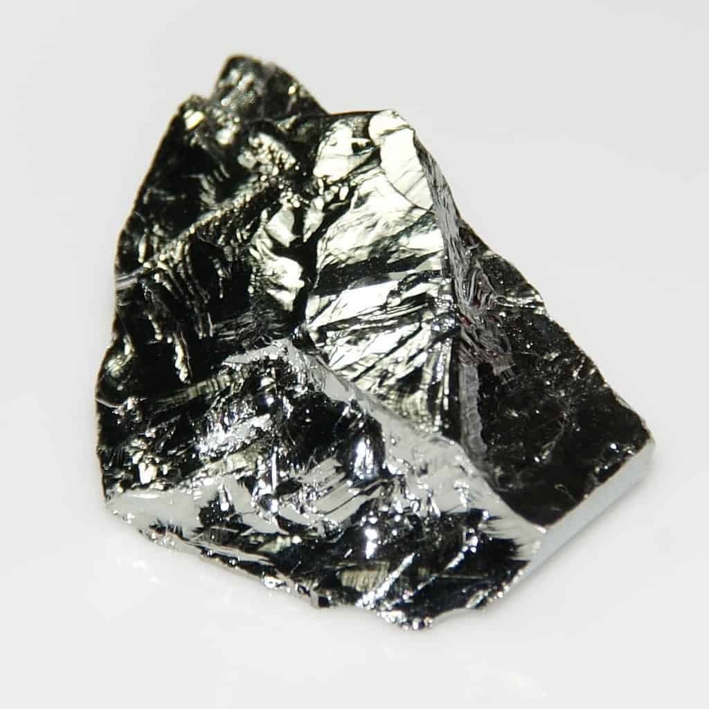
    Germanium is a chemical element with atomic number 32 which means there are 32 protons and 32 electrons in the atomic structure. The chemical symbol for Germanium is Ge. Germanium is a lustrous, hard, grayish-white metalloid in the carbon group, chemically similar to its group neighbors tin and silicon. Pure germanium is a semiconductor with an appearance similar to elemental silicon.

  • Germanium is more efficient than silicon for radiation detection due to its atomic number being much higher than silicon and due to lower average energy necessary to create an electron-hole pair, which is 3.6 eV for silicon and 2.9 eV for germanium. This provides the latter a better resolution in energy.
  • The FWHM for germanium detectors is a function of energy. For a 1.3 MeV photon, the FWHM is 2.1 keV, which is very low.
  • On the other hand, germanium has a small band gap energy (Egap = 0.67 eV), which requires to operate the detector at cryogenic temperatures. At room temperatures the noise caused by thermal excitation is very high.
  • semiconductor detectors - table of parametersThe average energy for creation of electron-hole pair is 2.9 eV. This value is approximately 10 times lower compared to the ionization energy of gases used in proportional chambers, drift chambers and etc. And it leads to massive creation of charge carriers.
  • Germanium has a high density of  5.323 g/cm3, which also increases the average energy loss per unit of length.
  • The detectors detectors are mechanically rigid and therefore no special supporting structures are needed.

Application of Germanium Detectors – Gamma Spectroscopy

As was written, the study and analysis of gamma ray spectra for scientific and technical use is called gamma spectroscopy, and gamma ray spectrometers are the instruments which observe and collect such data. A gamma ray spectrometer (GRS) is a sophisticated device for measuring the energy distribution of gamma radiation. For the measurement of gamma rays above several hundred keV, there are two detector categories of major importance, inorganic scintillators as NaI(Tl) and semiconductor detectors. In the previous articles, we described the gamma spectroscopy using scintillation detector, which consists of a suitable scintillator crystal, a photomultiplier tube, and a circuit for measuring the height of the pulses produced by the photomultiplier. The advantages of a scintillation counter are its efficiency (large size and high density) and the high precision and counting rates that are possible. Due to the high atomic number of iodine, a large number of all interactions will result in complete absorption of gamma-ray energy, so the photo fraction will be high.

HPGe Detector spectrum
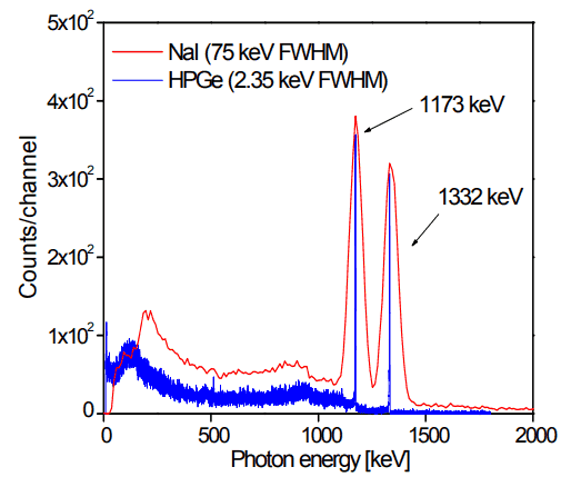
Figure: Caption: Comparison of NaI(Tl) and HPGe spectra for cobalt-60. Source: Radioisotopes and Radiation Methodology I, II. Soo Hyun Byun, Lecture Notes. McMaster University, Canada.

But if a perfect energy resolution is required, we have to use germanium-based detector, such as the HPGe detector. Germanium-based semiconductor detectors are most commonly used where a very good energy resolution is required, especially for gamma spectroscopy, as well as x-ray spectroscopy. In gamma spectroscopy, germanium is preferred due to its atomic number being much higher than silicon and which increases the probability of gamma ray interaction. Moreover, germanium has lower average energy necessary to create an electron-hole pair, which is 3.6 eV for silicon and 2.9 eV for germanium. This also provides the latter a better resolution in energy. The FWHM (full width at half maximum) for germanium detectors is a function of energy. For a 1.3 MeV photon, the FWHM is 2.1 keV, which is very low.

References:

Radiation Protection:

  1. Knoll, Glenn F., Radiation Detection and Measurement 4th Edition, Wiley, 8/2010. ISBN-13: 978-0470131480.
  2. Stabin, Michael G., Radiation Protection and Dosimetry: An Introduction to Health Physics, Springer, 10/2010. ISBN-13: 978-1441923912.
  3. Martin, James E., Physics for Radiation Protection 3rd Edition, Wiley-VCH, 4/2013. ISBN-13: 978-3527411764.
  4. U.S.NRC, NUCLEAR REACTOR CONCEPTS
  5. U.S. Department of Energy, Instrumantation and Control. DOE Fundamentals Handbook, Volume 2 of 2. June 1992.

Nuclear and Reactor Physics:

  1. J. R. Lamarsh, Introduction to Nuclear Reactor Theory, 2nd ed., Addison-Wesley, Reading, MA (1983).
  2. J. R. Lamarsh, A. J. Baratta, Introduction to Nuclear Engineering, 3d ed., Prentice-Hall, 2001, ISBN: 0-201-82498-1.
  3. W. M. Stacey, Nuclear Reactor Physics, John Wiley & Sons, 2001, ISBN: 0- 471-39127-1.
  4. Glasstone, Sesonske. Nuclear Reactor Engineering: Reactor Systems Engineering, Springer; 4th edition, 1994, ISBN: 978-0412985317
  5. W.S.C. Williams. Nuclear and Particle Physics. Clarendon Press; 1 edition, 1991, ISBN: 978-0198520467
  6. G.R.Keepin. Physics of Nuclear Kinetics. Addison-Wesley Pub. Co; 1st edition, 1965
  7. Robert Reed Burn, Introduction to Nuclear Reactor Operation, 1988.
  8. U.S. Department of Energy, Nuclear Physics and Reactor Theory. DOE Fundamentals Handbook, Volume 1 and 2. January 1993.
  9. Paul Reuss, Neutron Physics. EDP Sciences, 2008. ISBN: 978-2759800414.

See also:

Semiconductors

We hope, this article, Germanium-based Semiconductor Detector, helps you. If so, give us a like in the sidebar. Main purpose of this website is to help the public to learn some interesting and important information about radiation and dosimeters.

What is Semiconductor Material – Pure and Doped Semiconductor – Definition

There are many semiconductor materials in nature and others synthesized in laboratories. Pure Semiconductor vs Doped Semiconductor. The best known are silicon (Si) and germanium (Ge). Radiation Dosimetry
silicon strip detector - semiconductors
Silicin Strip Detector Source: micronsemiconductor.co.uk

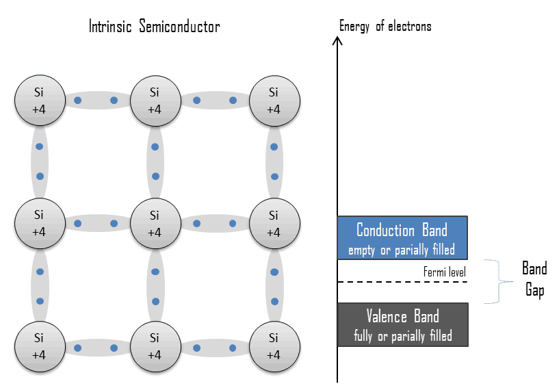
In general, semiconductors are materials, inorganic or organic, which have the ability to control their conduction depending on chemical structure, temperature, illumination, and presence of dopants. The name semiconductor comes from the fact that these materials  have an electrical conductivity between that of a metal, like copper, gold, etc. and an insulator, such as glass. They have an energy gap less than 4eV (about 1eV). In solid-state physics, this energy gap or band gap is an energy range between valence band and conduction band where electron states are forbidden. In contrast to conductors, electrons in a semiconductor must obtain energy (e.g. from ionizing radiation) to cross the band gap and to reach the conduction band. Properties of semiconductors are determined by the energy gap between valence and conduction bands.

Semiconductor Materials

There are many types of semiconductors in nature and others synthesized in laboratories; however, the best known are silicon (Si) and germanium (Ge).

Types of semiconductors:

  • silicon - semiconducting material
    Purified silicon. Source: wikipedia.org License: Public Domain

    Silicon. Silicon is a chemical element with atomic number 14 which means there are 14 protons and 14 electrons in the atomic structure. The chemical symbol for Silicon is Si. Silicon is a hard and brittle crystalline solid with a blue-grey metallic lustre, it is a tetravalent metalloid and semiconductor. Silicon is mainly used for charged particle detectors (especially for tracking charged particles) and soft X-ray detectors. The large band-gap energy (Egap= 1.12 eV) allows us to operate the detector at room temperature, but cooling is prefered to reduce noise. Silicon based detectors are very important in high-energy physics. Since silicon-based detectors are very good for tracking charged particles, they constitute a substantial part of detection system at the LHC in CERN.

  • Germanium - semiconductor
    12 grams polycrystalline germanium. Source: wikipedia.org License: CC BY 3.0

    Germanium. Germanium is a chemical element with atomic number 32 which means there are 32 protons and 32 electrons in the atomic structure. The chemical symbol for Germanium is Ge. Germanium is a lustrous, hard, grayish-white metalloid in the carbon group, chemically similar to its group neighbors tin and silicon. Pure germanium is a semiconductor with an appearance similar to elemental silicon.  Germanium is widely used for gamma ray spectroscopy. In gamma spectroscopy, germanium is preferred due to its atomic number being much higher than silicon and which increases the probability of gamma ray interaction. Germanium is more used than silicon for radiation detection because the average energy necessary to create an electron-hole pair is 3.6 eV for silicon and 2.9 eV for germanium, which provides the latter a better resolution in energy. On the other hand, germanium has a small band gap energy (Egap = 0.67 eV), which requires to operate the detector at cryogenic temperatures.

  • Diamond. Diamond is a solid form of the element carbon with its atoms arranged in a crystal structure called diamond cubic. Diamonds are also very good electrical insulators which strangely is both useful and problematic for electrical devices. Diamond is a wide-band gap semiconductor (Egap= 5.47 eV) with high potential as an electronic device material in many devices. Diamond detectors have many similarities with silicon detectors, but are expected to offer significant advantages, in particular a high radiation hardness and very low drift currents.
  • semiconductor detectors - table of parametersCdTe and CdZnTe. Cadmium telluride (CdTe) and cadmium zinc telluride (CdZnTe) have been regarded as promising semiconductor materials for hard X-ray and gamma ray detection. The high atomic number and the high density of these materials mean they can effectively attenuate X-rays and gamma rays with energies of greater than 20 keV that traditional silicon-based sensors are unable to detect. This significantly increases their quantum efficiency in comparison with silicon-based . The large band-gap energy (Egap= 1.44 eV) allows us to operate the detector at room temperature. On the other hand, a considerable amount of charge loss in these detectors produces a reduced energy resolution.

Pure Semiconductor

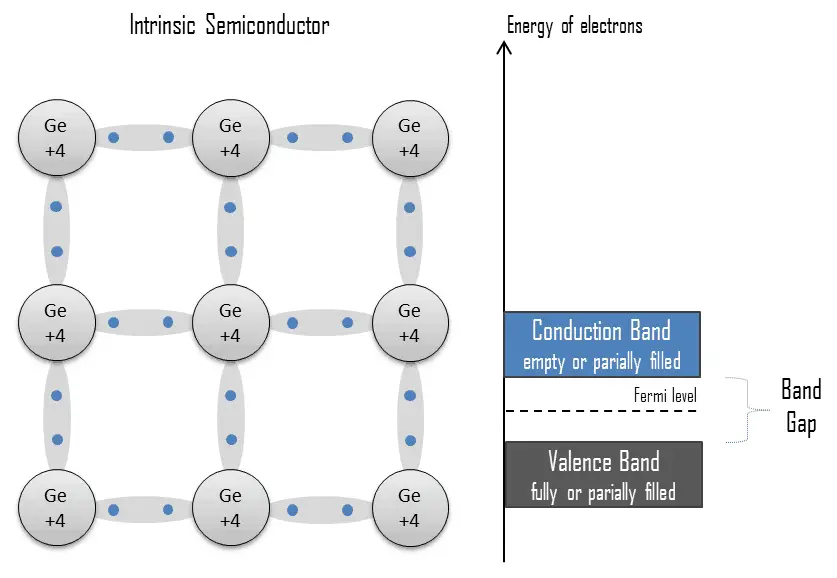
An intrinsic semiconductor is completely pure semiconductor without any significant dopant species present. Therefore, intrinsic semiconductors are also known as pure semiconductors or i-type semiconductors.

intrinsic semiconductorsThe number of charge carriers at certain temperature is therefore determined by the properties of the material itself instead of the amount of impurities. Note that, a 1 cm3 sample of pure germanium at 20 °C contains about 4.2×10²² atoms, but also contains about 2.5 x 10¹³ free electrons and 2.5 x 10¹³ holes. These charge carriers are produced by thermal excitation. In intrinsic semiconductors, the number of excited electrons and the number of holes are equal: n = p. Electrons and holes are created by excitation of electron from valence band to the conduction band. An electron hole (often simply called a hole) is the lack of an electron at a position where one could exist in an atom or atomic lattice. This equality may even be the case after doping the semiconductor, though only if it is doped with both donors and acceptors equally. In this case, n = p still holds, and the semiconductor remains intrinsic, though doped.

Semiconductors have an energy gap less than 4eV (about 1eV). Band gaps are naturally different for different materials. For example, diamond is a wide-band gap semiconductor (Egap= 5.47 eV) with high potential as an electronic device material in many devices. On the other side, germanium has a small band gap energy (Egap = 0.67 eV), which requires to operate the detector at cryogenic temperatures. In solid-state physics, this energy gap or band gap is an energy range between valence band and conduction band where electron states are forbidden. In contrast to conductors, electrons in a semiconductor must obtain energy (e.g. from ionizing radiation) to cross the band gap and to reach the conduction band.

Intrinsic semiconductors, however, are not very useful, as they are neither very good insulators nor very good conductors. However, one important feature of semiconductors is that their conductivity can be increased and controlled by doping with impurities and gating with electric fields. Recall, a 1 cm3 sample of pure germanium at 20 °C contains about 4.2×10²² atoms, but also contains about 2.5 x 10¹³ free electrons and 2.5 x 10¹³ holes constantly generated from thermal energy. Total absorption of a 1 MeV photon produces around 3 x 10⁵ electron-hole pairs. This value is minor in comparison the total number of free carriers in a 1 cm3 intrinsic semiconductor. As can be seen, the signal to noise ratio (S/N) would be minimal. The addition of 0.001% of arsenic (an impurity) donates an extra 1017 free electrons in the same volume and the electrical conductivity is increased by a factor of 10,000. In doped material the signal to noise ratio (S/N) would be even smaller. Because germanium has relatively low band gap, these detectors must be cooled in order to reduce the thermal generation of charge carriers to an acceptable level. Otherwise, leakage current induced noise destroys the energy resolution of the detector. Doping and gating move either the conduction or valence band much closer to the Fermi level, and greatly increase the number of partially filled states.

Doped Semiconductors

An extrinsic semiconductor, or doped semiconductor, is a semiconductor, that was intentionally doped for the purpose of modulating its electrical, optical and structural properties. In case of semiconductor detectors of ionizing radiation, doping is the intentional introduction of impurities into an intrinsic semiconductor for the purpose of changes in their electrical properties. Therefore, intrinsic semiconductors are also known as pure semiconductors or i-type semiconductors.

The addition of a small percentage of foreign atoms in the regular crystal lattice of silicon or germanium produces dramatic changes in their electrical properties, since these foreign atoms incorporated into the crystal structure of the semiconductor provide free charge carriers (electrons or electron holes) in the semiconductor. In an extrinsic semiconductor it is these foreign dopant atoms in the crystal lattice that mainly provide the charge carriers which carry electric current through the crystal. In general, there are two types of dopant atoms resulting in two types of extrinsic semiconductors. These dopants that produce the desired controlled changes are classified as either electron acceptors or donors and the corresponding doped semiconductors are known as:

Extrinsic semiconductors are components of many common electrical devices, as well of many detectors of ionizing radiation. For these purpose, a semiconductor diode (devices that allow current in only one direction) usually consists of p-type and n-type semiconductors placed in junction with one another.

References:

Radiation Protection:

  1. Knoll, Glenn F., Radiation Detection and Measurement 4th Edition, Wiley, 8/2010. ISBN-13: 978-0470131480.
  2. Stabin, Michael G., Radiation Protection and Dosimetry: An Introduction to Health Physics, Springer, 10/2010. ISBN-13: 978-1441923912.
  3. Martin, James E., Physics for Radiation Protection 3rd Edition, Wiley-VCH, 4/2013. ISBN-13: 978-3527411764.
  4. U.S.NRC, NUCLEAR REACTOR CONCEPTS
  5. U.S. Department of Energy, Instrumantation and Control. DOE Fundamentals Handbook, Volume 2 of 2. June 1992.

Nuclear and Reactor Physics:

  1. J. R. Lamarsh, Introduction to Nuclear Reactor Theory, 2nd ed., Addison-Wesley, Reading, MA (1983).
  2. J. R. Lamarsh, A. J. Baratta, Introduction to Nuclear Engineering, 3d ed., Prentice-Hall, 2001, ISBN: 0-201-82498-1.
  3. W. M. Stacey, Nuclear Reactor Physics, John Wiley & Sons, 2001, ISBN: 0- 471-39127-1.
  4. Glasstone, Sesonske. Nuclear Reactor Engineering: Reactor Systems Engineering, Springer; 4th edition, 1994, ISBN: 978-0412985317
  5. W.S.C. Williams. Nuclear and Particle Physics. Clarendon Press; 1 edition, 1991, ISBN: 978-0198520467
  6. G.R.Keepin. Physics of Nuclear Kinetics. Addison-Wesley Pub. Co; 1st edition, 1965
  7. Robert Reed Burn, Introduction to Nuclear Reactor Operation, 1988.
  8. U.S. Department of Energy, Nuclear Physics and Reactor Theory. DOE Fundamentals Handbook, Volume 1 and 2. January 1993.
  9. Paul Reuss, Neutron Physics. EDP Sciences, 2008. ISBN: 978-2759800414.

See also:

Types of Semiconductors

We hope, this article, Semiconductor Material – Pure and Doped Semiconductor, helps you. If so, give us a like in the sidebar. Main purpose of this website is to help the public to learn some interesting and important information about radiation and dosimeters.
What is Intrinsic and Extrinsic Semiconductor – Definition

An intrinsic semiconductor is completely pure semiconductor without any significant dopant species present. Intrinsic and Extrinsic Semiconductor
silicon strip detector - semiconductors
Silicin Strip Detector Source: micronsemiconductor.co.uk

In general, semiconductors are materials, inorganic or organic, which have the ability to control their conduction depending on chemical structure, temperature, illumination, and presence of dopants. The name semiconductor comes from the fact that these materials  have an electrical conductivity between that of a metal, like copper, gold, etc. and an insulator, such as glass. They have an energy gap less than 4eV (about 1eV). In solid-state physics, this energy gap or band gap is an energy range between valence band and conduction band where electron states are forbidden. In contrast to conductors, electrons in a semiconductor must obtain energy (e.g. from ionizing radiation) to cross the band gap and to reach the conduction band. Properties of semiconductors are determined by the energy gap between valence and conduction bands.

Intrinsic and Extrinsic Semiconductor

Intrinsic Semiconductor

An intrinsic semiconductor is completely pure semiconductor without any significant dopant species present. Therefore, intrinsic semiconductors are also known as pure semiconductors or i-type semiconductors.

intrinsic semiconductorsThe number of charge carriers at certain temperature is therefore determined by the properties of the material itself instead of the amount of impurities. Note that, a 1 cm3 sample of pure germanium at 20 °C contains about 4.2×10²² atoms, but also contains about 2.5 x 10¹³ free electrons and 2.5 x 10¹³ holes. These charge carriers are produced by thermal excitation. In intrinsic semiconductors, the number of excited electrons and the number of holes are equal: n = p. Electrons and holes are created by excitation of electron from valence band to the conduction band. An electron hole (often simply called a hole) is the lack of an electron at a position where one could exist in an atom or atomic lattice. This equality may even be the case after doping the semiconductor, though only if it is doped with both donors and acceptors equally. In this case, n = p still holds, and the semiconductor remains intrinsic, though doped.

Semiconductors have an energy gap less than 4eV (about 1eV). Band gaps are naturally different for different materials. For example, diamond is a wide-band gap semiconductor (Egap= 5.47 eV) with high potential as an electronic device material in many devices. On the other side, germanium has a small band gap energy (Egap = 0.67 eV), which requires to operate the detector at cryogenic temperatures. In solid-state physics, this energy gap or band gap is an energy range between valence band and conduction band where electron states are forbidden. In contrast to conductors, electrons in a semiconductor must obtain energy (e.g. from ionizing radiation) to cross the band gap and to reach the conduction band.

Extrinsic Semiconductors

An extrinsic semiconductor, or doped semiconductor, is a semiconductor, that was intentionally doped for the purpose of modulating its electrical, optical and structural properties. In case of semiconductor detectors of ionizing radiation, doping is the intentional introduction of impurities into an intrinsic semiconductor for the purpose of changes in their electrical properties. Therefore, intrinsic semiconductors are also known as pure semiconductors or i-type semiconductors.

The addition of a small percentage of foreign atoms in the regular crystal lattice of silicon or germanium produces dramatic changes in their electrical properties, since these foreign atoms incorporated into the crystal structure of the semiconductor provide free charge carriers (electrons or electron holes) in the semiconductor. In an extrinsic semiconductor it is these foreign dopant atoms in the crystal lattice that mainly provide the charge carriers which carry electric current through the crystal. In general, there are two types of dopant atoms resulting in two types of extrinsic semiconductors. These dopants that produce the desired controlled changes are classified as either electron acceptors or donors and the corresponding doped semiconductors are known as:

Extrinsic semiconductors are components of many common electrical devices, as well of many detectors of ionizing radiation. For these purpose, a semiconductor diode (devices that allow current in only one direction) usually consists of p-type and n-type semiconductors placed in junction with one another.

References:

Radiation Protection:

  1. Knoll, Glenn F., Radiation Detection and Measurement 4th Edition, Wiley, 8/2010. ISBN-13: 978-0470131480.
  2. Stabin, Michael G., Radiation Protection and Dosimetry: An Introduction to Health Physics, Springer, 10/2010. ISBN-13: 978-1441923912.
  3. Martin, James E., Physics for Radiation Protection 3rd Edition, Wiley-VCH, 4/2013. ISBN-13: 978-3527411764.
  4. U.S.NRC, NUCLEAR REACTOR CONCEPTS
  5. U.S. Department of Energy, Instrumantation and Control. DOE Fundamentals Handbook, Volume 2 of 2. June 1992.

Nuclear and Reactor Physics:

  1. J. R. Lamarsh, Introduction to Nuclear Reactor Theory, 2nd ed., Addison-Wesley, Reading, MA (1983).
  2. J. R. Lamarsh, A. J. Baratta, Introduction to Nuclear Engineering, 3d ed., Prentice-Hall, 2001, ISBN: 0-201-82498-1.
  3. W. M. Stacey, Nuclear Reactor Physics, John Wiley & Sons, 2001, ISBN: 0- 471-39127-1.
  4. Glasstone, Sesonske. Nuclear Reactor Engineering: Reactor Systems Engineering, Springer; 4th edition, 1994, ISBN: 978-0412985317
  5. W.S.C. Williams. Nuclear and Particle Physics. Clarendon Press; 1 edition, 1991, ISBN: 978-0198520467
  6. G.R.Keepin. Physics of Nuclear Kinetics. Addison-Wesley Pub. Co; 1st edition, 1965
  7. Robert Reed Burn, Introduction to Nuclear Reactor Operation, 1988.
  8. U.S. Department of Energy, Nuclear Physics and Reactor Theory. DOE Fundamentals Handbook, Volume 1 and 2. January 1993.
  9. Paul Reuss, Neutron Physics. EDP Sciences, 2008. ISBN: 978-2759800414.

See also:

Types of Semiconductors

We hope, this article, Intrinsic and Extrinsic Semiconductor, helps you. If so, give us a like in the sidebar. Main purpose of this website is to help the public to learn some interesting and important information about radiation and dosimeters.
What is Silicon Detector – Principle of Operation – Definition

Principle of Operation of Silicon Detectors. The operation of semiconductor detectors is  summarized in the following points. Ionizing radiation enters the sensitive volume of the detector …. Radiation Dosimetry
silicon strip detector - semiconductors
Silicin Strip Detector Source: micronsemiconductor.co.uk

Silicon-based semiconductor detectors are mainly used for charged particle detectors (especially for tracking charged particles) and soft X-ray detectors while germanium is widely used for gamma ray spectroscopy. A large, clean and almost perfect semiconductor is ideal as a counter for radioactivity. However, it is difficult to make large crystals with sufficient purity. The semiconductor detectors have, therefore, low efficiency, but they do give a very precise measure of the energy. Detectors based on silicon have sufficiently low noise even by room temperature. This is caused by the large band gap of silicon (Egap= 1.12 eV), which allows us to operate the detector at room temperature, but cooling is prefered to reduce noise. The drawback is that silicon detectors are much more expensive than cloud chambers or wire chambers and require sophisticated cooling to reduce leakage currents (noise). They also suffer degradation over time from radiation, however this can be greatly reduced thanks to the Lazarus effect.

Principle of Operation of Silicon Detectors  

The operation of semiconductor detectors is  summarized in the following points:

  • Ionizing radiation enters the sensitive volume of the detector and interacts with the semiconductor material.
  • Particle passing through the detector ionizes the atoms of semiconductor, producing the electron-hole pairs. The number of electron-hole pairs is proportional to the energy of the radiation to the semiconductor. As a result, a number of electrons are transferred from the valence band to the conduction band, and an equal number of holes are created in the valence band.
  • Under the influence of an electric field, electrons and holes travel to the electrodes, where they result in a pulse that can be measured in an outer circuit,
  • This pulse carries information about the energy of the original incident radiation. The number of such pulses per unit time also gives information about the intensity of the radiation.

The energy required to produce electron-hole-pairs is very low compared to the energy required to produce paired ions in a gaseous ionization detector. In semiconductor detectors the statistical variation of the pulse height is smaller and the energy resolution is higher. As the electrons travel fast, the time resolution is also very good. Compared with gaseous ionization detectors, the density of a semiconductor detector is very high, and charged particles of high energy can give off their energy in a semiconductor of relatively small dimensions.

References:

Radiation Protection:

  1. Knoll, Glenn F., Radiation Detection and Measurement 4th Edition, Wiley, 8/2010. ISBN-13: 978-0470131480.
  2. Stabin, Michael G., Radiation Protection and Dosimetry: An Introduction to Health Physics, Springer, 10/2010. ISBN-13: 978-1441923912.
  3. Martin, James E., Physics for Radiation Protection 3rd Edition, Wiley-VCH, 4/2013. ISBN-13: 978-3527411764.
  4. U.S.NRC, NUCLEAR REACTOR CONCEPTS
  5. U.S. Department of Energy, Instrumantation and Control. DOE Fundamentals Handbook, Volume 2 of 2. June 1992.

Nuclear and Reactor Physics:

  1. J. R. Lamarsh, Introduction to Nuclear Reactor Theory, 2nd ed., Addison-Wesley, Reading, MA (1983).
  2. J. R. Lamarsh, A. J. Baratta, Introduction to Nuclear Engineering, 3d ed., Prentice-Hall, 2001, ISBN: 0-201-82498-1.
  3. W. M. Stacey, Nuclear Reactor Physics, John Wiley & Sons, 2001, ISBN: 0- 471-39127-1.
  4. Glasstone, Sesonske. Nuclear Reactor Engineering: Reactor Systems Engineering, Springer; 4th edition, 1994, ISBN: 978-0412985317
  5. W.S.C. Williams. Nuclear and Particle Physics. Clarendon Press; 1 edition, 1991, ISBN: 978-0198520467
  6. G.R.Keepin. Physics of Nuclear Kinetics. Addison-Wesley Pub. Co; 1st edition, 1965
  7. Robert Reed Burn, Introduction to Nuclear Reactor Operation, 1988.
  8. U.S. Department of Energy, Nuclear Physics and Reactor Theory. DOE Fundamentals Handbook, Volume 1 and 2. January 1993.
  9. Paul Reuss, Neutron Physics. EDP Sciences, 2008. ISBN: 978-2759800414.

See also:

Silicon Detectors

We hope, this article, Silicon Detector – Principle of Operation, helps you. If so, give us a like in the sidebar. Main purpose of this website is to help the public to learn some interesting and important information about radiation and dosimeters.
What is Application of Silicon Detectors – Definition

Application of Silicon Detectors. Since silicon-based detectors are very good for tracking charged particles, they constitute a substantial part of detection system at the LHC in CERN. Radiation Dosimetry
silicon strip detector - semiconductors
Silicin Strip Detector Source: micronsemiconductor.co.uk

Silicon-based semiconductor detectors are mainly used for charged particle detectors (especially for tracking charged particles) and soft X-ray detectors while germanium is widely used for gamma ray spectroscopy. A large, clean and almost perfect semiconductor is ideal as a counter for radioactivity. However, it is difficult to make large crystals with sufficient purity. The semiconductor detectors have, therefore, low efficiency, but they do give a very precise measure of the energy. Detectors based on silicon have sufficiently low noise even by room temperature. This is caused by the large band gap of silicon (Egap= 1.12 eV), which allows us to operate the detector at room temperature, but cooling is prefered to reduce noise. The drawback is that silicon detectors are much more expensive than cloud chambers or wire chambers and require sophisticated cooling to reduce leakage currents (noise). They also suffer degradation over time from radiation, however this can be greatly reduced thanks to the Lazarus effect.

Application of Silicon Detectors

Since silicon-based detectors are very good for tracking charged particles, they constitute a substantial part of detection system at the LHC in CERN. Most silicon particle detectors work, in principle, by doping narrow (usually around 100 micrometers wide) strips of silicon to turn them into diodes, which are then reverse biased. As charged particles pass through these strips, they cause small ionization currents that can be detected and measured. Arranging thousands of these detectors around a collision point in a particle accelerator can yield an accurate picture of what paths particles take. For example, the Inner Tracking System (ITS) of a Large Ion Collider Experiment (ALICE) contains three layers of silicon-based detectors:

  • Silicon Pixel Detector (SPD)
  • Silicon Drift Detector (SDD)
  • Silicon Strip Detector (SSD)

Silicon Strip Detectors

Silicon-based detectors are very good for tracking charged particles. A silicon strip detector is an arrangement of strip like shaped implants acting as charge collecting electrodes.

Silicon strip detectors 5 x 5 cm2 in area are quite common and are used in series (just like planes of MWPCs) to determine charged-particle trajectories to position-accuracies of the order of several μm in the transverse direction.  Placed on a low doped fully depleted silicon wafer these implants form a one-dimensional array of diodes. By connecting each of the metalized strips to a charge sensitive amplifier a position sensitive detector is built. Two dimensional position measurements can be achieved by applying an additional strip like doping on the wafer backside by use of a double sided technology.  Such devices can be used to measure small impact parameters and thereby determine whether some charged particle originated from a primary collision or was the decay product of a primary particle that traveled a small distance from the original interaction, and then decayed.

Silicon strip detectors constitute a substantial part of detection system at the LHC in CERN. Most silicon particle detectors work, in principle, by doping narrow (usually around 100 micrometers wide) strips of silicon to turn them into diodes, which are then reverse biased. As charged particles pass through these strips, they cause small ionization currents that can be detected and measured. Arranging thousands of these detectors around a collision point in a particle accelerator can yield an accurate picture of what paths particles take.

For example, the Inner Tracking System (ITS) of a Large Ion Collider Experiment (ALICE) contains three layers of silicon-based detectors:

  • Silicon Pixel Detector (SPD)
  • Silicon Drift Detector (SDD)
  • Silicon Strip Detector (SSD)

Delta E – E Detector – Telescope

delta E - E Telescope - chart
Example of histogram from ΔE-E detector. Each hyperbola-like curve represents different particle in the beam.

In experimental physics, ΔE-E detectors, known as telescopes, are powerful devices for charged particles identification. In order to provide charged-particle identification, telescopes consisting of pairs of thin and thick surface-barrier detectors can be used. These detectors must be positioned in series. The velocity is deduced from the stopping power measured in the thin detectors (ΔE detectors). There is a strong correlation between the energy deposited in each detector. This correlation depends on the mass (A), the charge (Z) and the kinetic energy (E) of each particle. The mass is deduced from the range or from the total kinetic energy loss in the thicker detector (E detector).

Telescopes can be  composed of several detectors (ionization chambers, silicon detectors and scintillators for instance) stacked in order to slow down incident charged particles, the first detector being the thinnest and the last one the thickest. CsI scintillation counters can be, for example used as final E counters. As an example of telescope, an assembly based on two front ΔE silicon detectors (10 or 30 µm) and an E silicon counter 1500 µm thick may be used for detection of high-energy charged particles.

References:

Radiation Protection:

  1. Knoll, Glenn F., Radiation Detection and Measurement 4th Edition, Wiley, 8/2010. ISBN-13: 978-0470131480.
  2. Stabin, Michael G., Radiation Protection and Dosimetry: An Introduction to Health Physics, Springer, 10/2010. ISBN-13: 978-1441923912.
  3. Martin, James E., Physics for Radiation Protection 3rd Edition, Wiley-VCH, 4/2013. ISBN-13: 978-3527411764.
  4. U.S.NRC, NUCLEAR REACTOR CONCEPTS
  5. U.S. Department of Energy, Instrumantation and Control. DOE Fundamentals Handbook, Volume 2 of 2. June 1992.

Nuclear and Reactor Physics:

  1. J. R. Lamarsh, Introduction to Nuclear Reactor Theory, 2nd ed., Addison-Wesley, Reading, MA (1983).
  2. J. R. Lamarsh, A. J. Baratta, Introduction to Nuclear Engineering, 3d ed., Prentice-Hall, 2001, ISBN: 0-201-82498-1.
  3. W. M. Stacey, Nuclear Reactor Physics, John Wiley & Sons, 2001, ISBN: 0- 471-39127-1.
  4. Glasstone, Sesonske. Nuclear Reactor Engineering: Reactor Systems Engineering, Springer; 4th edition, 1994, ISBN: 978-0412985317
  5. W.S.C. Williams. Nuclear and Particle Physics. Clarendon Press; 1 edition, 1991, ISBN: 978-0198520467
  6. G.R.Keepin. Physics of Nuclear Kinetics. Addison-Wesley Pub. Co; 1st edition, 1965
  7. Robert Reed Burn, Introduction to Nuclear Reactor Operation, 1988.
  8. U.S. Department of Energy, Nuclear Physics and Reactor Theory. DOE Fundamentals Handbook, Volume 1 and 2. January 1993.
  9. Paul Reuss, Neutron Physics. EDP Sciences, 2008. ISBN: 978-2759800414.

See also:

Silicon Detectors

We hope, this article, Application of Silicon Detectors, helps you. If so, give us a like in the sidebar. Main purpose of this website is to help the public to learn some interesting and important information about radiation and dosimeters.
What is Advantage and Disadvantage of Silicon Detectors – Definition

Advantages and Disadvantages of Silicon Detectors. Silicon detectors are very good for tracking charged particles. On the other hand, they are very expensive. Radiation Dosimetry
silicon strip detector - semiconductors
Silicin Strip Detector Source: micronsemiconductor.co.uk

Silicon-based semiconductor detectors are mainly used for charged particle detectors (especially for tracking charged particles) and soft X-ray detectors while germanium is widely used for gamma ray spectroscopy. A large, clean and almost perfect semiconductor is ideal as a counter for radioactivity. However, it is difficult to make large crystals with sufficient purity. The semiconductor detectors have, therefore, low efficiency, but they do give a very precise measure of the energy. Detectors based on silicon have sufficiently low noise even by room temperature. This is caused by the large band gap of silicon (Egap= 1.12 eV), which allows us to operate the detector at room temperature, but cooling is prefered to reduce noise.

Advantages and Disadvantages of Silicon Detectors

Advantages of Silicon Detectors

  • Compared with gaseous ionization detectors, the density of a semiconductor detector is very high, and charged particles of high energy can give off their energy in a semiconductor of relatively small dimensions.
  • Silicon has a high density of  2.329 g/cm3 and therefore the average energy loss per unit of length allows building thin detectors (e.g. 300 µm) that still produce measurable signals. For example, in case of minimum ionizing particle (MIP) the energy loss is 390 eV/µm. The silicon detectors are mechanically rigid and therefore no special supporting structures are needed.
  • Silicon-based detectors are very good for tracking charged particles, they constitute a substantial part of detection system at the LHC in CERN.
  • Silicon detectors can be used in strong magnetic fields.

Disadvantages of Silicon Detectors

  • Price. The disadvantage is that silicon detectors are much more expensive than cloud chambers or wire chambers.
  • Degradation. They also suffer degradation over time from radiation, however this can be greatly reduced thanks to the Lazarus effect.
  • High FWHM. In gamma spectroscopy, germanium is preferred due to its atomic number being much higher than silicon and which increases the probability of gamma ray interaction. Moreover, germanium has lower average energy necessary to create an electron-hole pair, which is 3.6 eV for silicon and 2.9 eV for germanium. This also provides the latter a better resolution in energy.
References:

Radiation Protection:

  1. Knoll, Glenn F., Radiation Detection and Measurement 4th Edition, Wiley, 8/2010. ISBN-13: 978-0470131480.
  2. Stabin, Michael G., Radiation Protection and Dosimetry: An Introduction to Health Physics, Springer, 10/2010. ISBN-13: 978-1441923912.
  3. Martin, James E., Physics for Radiation Protection 3rd Edition, Wiley-VCH, 4/2013. ISBN-13: 978-3527411764.
  4. U.S.NRC, NUCLEAR REACTOR CONCEPTS
  5. U.S. Department of Energy, Instrumantation and Control. DOE Fundamentals Handbook, Volume 2 of 2. June 1992.

Nuclear and Reactor Physics:

  1. J. R. Lamarsh, Introduction to Nuclear Reactor Theory, 2nd ed., Addison-Wesley, Reading, MA (1983).
  2. J. R. Lamarsh, A. J. Baratta, Introduction to Nuclear Engineering, 3d ed., Prentice-Hall, 2001, ISBN: 0-201-82498-1.
  3. W. M. Stacey, Nuclear Reactor Physics, John Wiley & Sons, 2001, ISBN: 0- 471-39127-1.
  4. Glasstone, Sesonske. Nuclear Reactor Engineering: Reactor Systems Engineering, Springer; 4th edition, 1994, ISBN: 978-0412985317
  5. W.S.C. Williams. Nuclear and Particle Physics. Clarendon Press; 1 edition, 1991, ISBN: 978-0198520467
  6. G.R.Keepin. Physics of Nuclear Kinetics. Addison-Wesley Pub. Co; 1st edition, 1965
  7. Robert Reed Burn, Introduction to Nuclear Reactor Operation, 1988.
  8. U.S. Department of Energy, Nuclear Physics and Reactor Theory. DOE Fundamentals Handbook, Volume 1 and 2. January 1993.
  9. Paul Reuss, Neutron Physics. EDP Sciences, 2008. ISBN: 978-2759800414.

See also:

Silicon Detectors

We hope, this article, Advantage and Disadvantage of Silicon Detectors, helps you. If so, give us a like in the sidebar. Main purpose of this website is to help the public to learn some interesting and important information about radiation and dosimeters.

What is Silicon Strip Detector – Definition

Silicon strip detectors are used in series (just like planes of MWPCs) to determine charged-particle trajectories to position-accuracies of the order of several μm in the transverse direction. Radiation Dosimetry
silicon strip detector - semiconductors
Silicin Strip Detector Source: micronsemiconductor.co.uk

Silicon-based detectors are very good for tracking charged particles. A silicon strip detector is an arrangement of strip like shaped implants acting as charge collecting electrodes.

Silicon strip detectors 5 x 5 cm2 in area are quite common and are used in series (just like planes of MWPCs) to determine charged-particle trajectories to position-accuracies of the order of several μm in the transverse direction.  Placed on a low doped fully depleted silicon wafer these implants form a one-dimensional array of diodes. By connecting each of the metalized strips to a charge sensitive amplifier a position sensitive detector is built. Two dimensional position measurements can be achieved by applying an additional strip like doping on the wafer backside by use of a double sided technology.  Such devices can be used to measure small impact parameters and thereby determine whether some charged particle originated from a primary collision or was the decay product of a primary particle that traveled a small distance from the original interaction, and then decayed.

Silicon strip detectors constitute a substantial part of detection system at the LHC in CERN. Most silicon particle detectors work, in principle, by doping narrow (usually around 100 micrometers wide) strips of silicon to turn them into diodes, which are then reverse biased. As charged particles pass through these strips, they cause small ionization currents that can be detected and measured. Arranging thousands of these detectors around a collision point in a particle accelerator can yield an accurate picture of what paths particles take.

For example, the Inner Tracking System (ITS) of a Large Ion Collider Experiment (ALICE) contains three layers of silicon-based detectors:

  • Silicon Pixel Detector (SPD)
  • Silicon Drift Detector (SDD)
  • Silicon Strip Detector (SSD)
References:

Radiation Protection:

  1. Knoll, Glenn F., Radiation Detection and Measurement 4th Edition, Wiley, 8/2010. ISBN-13: 978-0470131480.
  2. Stabin, Michael G., Radiation Protection and Dosimetry: An Introduction to Health Physics, Springer, 10/2010. ISBN-13: 978-1441923912.
  3. Martin, James E., Physics for Radiation Protection 3rd Edition, Wiley-VCH, 4/2013. ISBN-13: 978-3527411764.
  4. U.S.NRC, NUCLEAR REACTOR CONCEPTS
  5. U.S. Department of Energy, Instrumantation and Control. DOE Fundamentals Handbook, Volume 2 of 2. June 1992.

Nuclear and Reactor Physics:

  1. J. R. Lamarsh, Introduction to Nuclear Reactor Theory, 2nd ed., Addison-Wesley, Reading, MA (1983).
  2. J. R. Lamarsh, A. J. Baratta, Introduction to Nuclear Engineering, 3d ed., Prentice-Hall, 2001, ISBN: 0-201-82498-1.
  3. W. M. Stacey, Nuclear Reactor Physics, John Wiley & Sons, 2001, ISBN: 0- 471-39127-1.
  4. Glasstone, Sesonske. Nuclear Reactor Engineering: Reactor Systems Engineering, Springer; 4th edition, 1994, ISBN: 978-0412985317
  5. W.S.C. Williams. Nuclear and Particle Physics. Clarendon Press; 1 edition, 1991, ISBN: 978-0198520467
  6. G.R.Keepin. Physics of Nuclear Kinetics. Addison-Wesley Pub. Co; 1st edition, 1965
  7. Robert Reed Burn, Introduction to Nuclear Reactor Operation, 1988.
  8. U.S. Department of Energy, Nuclear Physics and Reactor Theory. DOE Fundamentals Handbook, Volume 1 and 2. January 1993.
  9. Paul Reuss, Neutron Physics. EDP Sciences, 2008. ISBN: 978-2759800414.

See also:

Silicon Detectors

We hope, this article, Silicon Strip Detector, helps you. If so, give us a like in the sidebar. Main purpose of this website is to help the public to learn some interesting and important information about radiation and dosimeters.