Germanium-based Semiconductor Detectors

Germanium-based semiconductor detectors are most commonly used where a very good energy resolution is required, especially for gamma spectroscopy, as well as x-ray spectroscopy. In gamma spectroscopy, germanium is preferred due to its atomic number being much higher than silicon and which increases the probability of gamma ray interaction. Moreover, germanium has lower average energy necessary to create an electron-hole pair, which is 3.6 eV for silicon and 2.9 eV for germanium. This also provides the latter a better resolution in energy. A large, clean and almost perfect germanium semiconductor is ideal as a counter for radioactivity. However, it is difficult and expensive to make large crystals with sufficient purity. While silicon-based detectors cannot be thicker than a few millimeters, germanium can have a depleted, sensitive thickness of centimeters, and therefore can be used as a total absorption detector for gamma rays up to few MeV.
On the other hand, in order to achieve maximum efficiency the detectors must operate at the very low temperatures of liquid nitrogen (-196°C), because at room temperatures the noise caused by thermal excitation is very high.
Since germanium detectors produce the highest resolution commonly available today, they are used to measure radiation in a variety of applications including personnel and environmental monitoring for radioactive contamination, medical applications, radiometric assay, nuclear security and nuclear plant safety.
Germanium Detector – Principle of Operation
The operation of semiconductor detectors is summarized in the following points:
- Ionizing radiation enters the sensitive volume (germanium crystal) of the detector and interacts with the semiconductor material.
- High-energy photon passing through the detector ionizes the atoms of semiconductor, producing the electron-hole pairs. The number of electron-hole pairs is proportional to the energy of the radiation to the semiconductor. As a result, a number of electrons are transferred from the valence band to the conduction band, and an equal number of holes are created in the valence band.
- Since germanium can have a depleted, sensitive thickness of centimeters, they are able to absorb high-energy photons totally (up to few MeV).
- Under the influence of an electric field, electrons and holes travel to the electrodes, where they result in a pulse that can be measured in an outer circuit.
- This pulse carries information about the energy of the original incident radiation. The number of such pulses per unit time also gives information about the intensity of the radiation.
In all cases, a photon deposits a portion of its energy along its path and can be absorbed totally. Total absorption of a 1 MeV photon produces around 3 x 10⁵ electron-hole pairs. This value is minor in comparison the total number of free carriers in a 1 cm3 intrinsic semiconductor. Particle passing through the detector ionizes the atoms of semiconductor, producing the electron-hole pairs. But in germanium-based detectors at room temperature, thermal excitation is dominant. It is caused by impurities, irregularity in structure lattice or by dopant. It strongly depends on the Egap (a distance between valence and conduction band), which is very low for germanium (Egap= 0.67 eV). Since thermal excitation results in the detector noise, active cooling is required for some types of semiconductors (e.g. germanium).
![]() Note that, a 1 cm3 sample of pure germanium at 20 °C contains about 4.2×10²² atoms, but also contains about 2.5 x 10¹³ free electrons and 2.5 x 10¹³ holes constantly generated from thermal energy. As can be seen, the signal to noise ratio (S/N) would be minimal (compare it with 3 x 10⁵ electron-hole pairs). The addition of 0.001% of arsenic (an impurity) donates an extra 1017 free electrons in the same volume and the electrical conductivity is increased by a factor of 10,000. In doped material the signal to noise ratio (S/N) would be even smaller. Because germanium has relatively low band gap, these detectors must be cooled in order to reduce the thermal generation of charge carriers (thus reverse leakage current) to an acceptable level. Otherwise, leakage current induced noise destroys the energy resolution of the detector.
Note that, a 1 cm3 sample of pure germanium at 20 °C contains about 4.2×10²² atoms, but also contains about 2.5 x 10¹³ free electrons and 2.5 x 10¹³ holes constantly generated from thermal energy. As can be seen, the signal to noise ratio (S/N) would be minimal (compare it with 3 x 10⁵ electron-hole pairs). The addition of 0.001% of arsenic (an impurity) donates an extra 1017 free electrons in the same volume and the electrical conductivity is increased by a factor of 10,000. In doped material the signal to noise ratio (S/N) would be even smaller. Because germanium has relatively low band gap, these detectors must be cooled in order to reduce the thermal generation of charge carriers (thus reverse leakage current) to an acceptable level. Otherwise, leakage current induced noise destroys the energy resolution of the detector.
Reverse Biased Junction
The semiconductor detector operates much better as a radiation detector if an external voltage is applied across the junction in the reverse biased direction. The depletion region will function as a radiation detector. Improvement can be reached by use of a reverse-bias voltage to the P-N junction to deplete the detector of free carriers, which is the principle of the most semiconductor detectors. Reverse biasing a junction increases the thickness of the depletion region because the potential difference across the junction is enhanced. Germanium detectors have a p-i-n structure in which the intrinsic (i) region is sensitive to ionizing radiation, particularly X rays and gamma rays. Under reverse bias, an electric field extends across the intrinsic or depleted region. In this case, negative voltage is applied to the p-side and positive to the second one. Holes in the p-region are attracted from the junction towards the p contact and similarly for electrons and the n contact. This charge, which is in proportion to the energy deposited in the detector by the incoming photon, is converted into a voltage pulse by an integral charge sensitive preamplifier.
See also: Germanium Detectors, MIRION Technologies. <available from: https://www.mirion.com/products/germanium-detectors>.
Application of Germanium Detectors – Gamma Spectroscopy
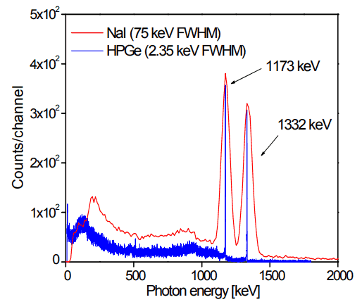
As was written, the study and analysis of gamma ray spectra for scientific and technical use is called gamma spectroscopy, and gamma ray spectrometers are the instruments which observe and collect such data. A gamma ray spectrometer (GRS) is a sophisticated device for measuring the energy distribution of gamma radiation. For the measurement of gamma rays above several hundred keV, there are two detector categories of major importance, inorganic scintillators as NaI(Tl) and semiconductor detectors. In the previous articles, we described the gamma spectroscopy using scintillation detector, which consists of a suitable scintillator crystal, a photomultiplier tube, and a circuit for measuring the height of the pulses produced by the photomultiplier. The advantages of a scintillation counter are its efficiency (large size and high density) and the high precision and counting rates that are possible. Due to the high atomic number of iodine, a large number of all interactions will result in complete absorption of gamma-ray energy, so the photo fraction will be high.

But if a perfect energy resolution is required, we have to use germanium-based detector, such as the HPGe detector. Germanium-based semiconductor detectors are most commonly used where a very good energy resolution is required, especially for gamma spectroscopy, as well as x-ray spectroscopy. In gamma spectroscopy, germanium is preferred due to its atomic number being much higher than silicon and which increases the probability of gamma ray interaction. Moreover, germanium has lower average energy necessary to create an electron-hole pair, which is 3.6 eV for silicon and 2.9 eV for germanium. This also provides the latter a better resolution in energy. The FWHM (full width at half maximum) for germanium detectors is a function of energy. For a 1.3 MeV photon, the FWHM is 2.1 keV, which is very low.
We hope, this article, Germanium-based Semiconductor Detector, helps you. If so, give us a like in the sidebar. Main purpose of this website is to help the public to learn some interesting and important information about radiation and dosimeters.
